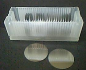
PAM-XIAMEN offers p type electronic grade Germanium (Ge) wafer. Germanium is a chemical element. Its chemical symbol is Ge. Its atomic number is 32 and the atomic weight is 72.64, belonging to the IVA group elements. So the germanium electron configuration must have 32 electrons. Owing to the excellent crystallographic properties and unique electrical properties of Ge wafer, thin germanium wafer is used in various applications, including MOS-devices, space solar cells, ground solar cells, sensors, infrared optics, high-brightness LEDs, nanoelectronic transtor application and many other semiconductor applications. You can buy thin germanium wafers in following specifications:
1. Single Crystal Thin Germanium Wafer Specifications (PAM190314-Ge)
Item 1:
| Item | P Type Thin Germanium Wafer |
| Size | 4” |
| Diameter | 100 +/-0.25 mm |
| Orientation | <100> off 6 or 9 degree toward <111> |
| Type / Dopant | P / Ga |
| Thickness | 175 +/- 10 um |
| Resistivity | (0.74-2.81)E-2 ohm-cm |
| Primary Flat Length | 32 +/-1mm |
| EPD | <= 300 cm-2 |
| BOW | <=10um |
| WARP | <=10um |
| TTV | <=15um |
| Front Surface | Polished |
| Back Surface | Etched |
| Edge Surface Finishing | Cylindrical ground |
| Surface Roughness ( Ra ) | <=5A |
| Epi Ready | Yes |
| Package | Single wafer container |
Mark: For surface process of thin germanium wafer, one side can be epi-ready polished for epitaxial growth and other side can be mirror-like polished for optical transmission.
Item 2: PAM210701-GE
| Item | Spec. | Unit |
| Growth Method | VGF | |
| Conductivity Type | S-C-P | |
| Resistivity | 0.005~0.03 | Ohm-cm |
| EPD | <300 | Counts/cm2 |
| Diameter | 150 ± 0.2 | mm |
| Thickness | 210~240 | um |
| Orientation | (100) 6° off towards (111) ± 0.5° | |
| Major Flat Orientation | <100> ± 0.2° | |
| Major Flat Length | 15 ± 1 | mm |
| Edge Radius | N/A | |
| Front Side Surface | Polished | |
| Back Side Surface | Diamond Ground | |
| Ingot CC | 2.000E+17~3.000E+18 | |
| TTV | ≤15 | um |
| Warp | ≤40 | um |
| Bow | ≤30 | um |
| Laser Mark | Opposite from primary flat | |
| Epi-ready | YES |
Item 3:
| Item | Undoped Ge Wafer |
| Size | 4” |
| Diameter | 100 +/-0.25 mm |
| Orientation | <100>+/-0.5deg. |
| Type / Dopant | Undoped |
| Thickness | 500+/- 10 um |
| Resistivity | >30 ohm-cm |
| Primary Flat Length | 32 +/-1mm |
| EPD | <= 10000 cm-2 |
| Front Surface | Polished |
| Back Surface | Etched |
| Edge Surface Finishing | Cylindrical ground |
| Surface Roughness ( Ra ) | <=5A |
| Epi Ready | Yes |
| Package | Single wafer container |
2. Germanium Properties
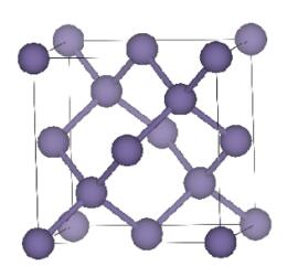
Germanium is a solid material and cannot react with oxygen at room temperature. Germanium hardness is not so high, so it is very brittle. Because of the the property of metal and non-metal, germanium has eletric conductivity. Germanium crystal structure diagram:
Germanium band gap is decreasing when the temperature goes up, please see highlited part in red circle:

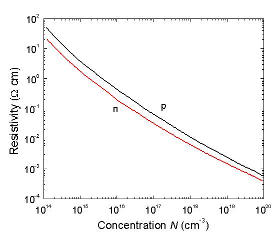
Following figure shows the relationship between germanium resistivity and impurity concentration:
3. Germanium Crystal Growth Research based on Solar Ge Wafer
Solar germanium wafers are mainly used in the construction of ground-based/space solar power stations, ultra-bright automotive LED lights, and charging devices for equipment, etc.. At present, the Czochralski method or vertical gradient solidification method is mainly used to manufacture thin germanium wafer. The main difference between CZ and VGF is that the CZ method is fast and highly controllable, but it is more difficult to grow low dislocation density germanium single crystals. A few semiconductor wafer companies, including PAM-XIAMEN, have independently designed and improved the thermal field system of the Czochralski germanium single crystal furnace to optimize the single crystal growth parameters, and can also grow qualified low-dislocation P-type germanium single crystals.
Dislocation density is one of the important parameters that determine the quality of crystal germanium wafer. Thermal stress and crystal temperature are the main factors affecting the dislocation density distribution in the crystal. In actual production, obtaining high-purity single crystal germanium substrates with low dislocation density is a problem in itself. In order to obtain low-dislocation germanium single crystals by CZ method, a company in Russia has conducted related research on the floating crucible method. The thermal field includes the main crucible and the additional floating inner crucible in the melt. Graphite felt insulation is used on the sides and bottom to keep warm. The main heater heats the germanium melt in the main crucible, and the sub heater located above the melt surface heats the periphery of the crystal. In addition, German researchers also proposed the no-crucible contact VGF method of germanium single crystal growth. Compared with conventionally grown germanium crystals, the separated grown crystals have superior structural perfection, and the dislocation value is more than an order of magnitude lower than that of attached grown crystals. This can be attributed to the absence of contact between the crucible wall and the crystal during the growth process, thereby reducing thermal stress and thermomechanical stress.
In short, controlling the Ge single crystal dislocation density is one significant way to ensure the high quality of the thin germanium wafer.
4. FAQ:
Q1: For Ge(211), I am still interested in it. Can you make 300um on Ge(211)?
A: Yes, PAM-XIAMEN can make the thickness of Ge(211) in 300um, but 400um thick will be better.
Q2: According to your comment that normally few to use Ge (111) on the resistivity of 5~40 ohm.cm, Ge (111) undoped (it is resistivity>40 ohm.cm) is much popular for optical application, so orientation <111> is undoped, is there a difference in transmission ?
A:Transmission of germanium (111) undoped is slight better than n type one.
Q3: For your “epi-ready” polishing Ge wafer, can we simply remove the oxide layer by thermal cleaning in ultra-high vacuum, e.g., at 500-600 degree Celsius, without any additional chemical process?
We will try a couple of more tests by putting your substrates and the other substrates together in the same run. Then we will decide where to purchase Ge wafer for our next round. The unit price of your wafer is slightly lower than the others but we need to be sure that they perform.
A: Yes, the epi-ready germanium wafer will be deoxidized at high temperature after entering the epitaxy furnace. The specific temperature depends on the setting of various equipment and the requirements of epitaxy process. However definitely our ge wafer would be same as the wafers from other suppliers in this point.
Q4: How to clean germanium wafers?
A: You need to wash the germanium plates in a hydromechanical washer using a certain material, while maintaining the integrity of the polished sides. After washing, the product must be dried by xx or xx. Washed plates should not have streaks, stains and dust particles with a particle size of> 0.2 um, in an amount of no more than 30 pcs. (201210)
For details about germanium cleaning, please send email to tech@powerwaywafer.com.

For more information, please contact us email at victorchan@powerwaywafer.com and powerwaymaterial@gmail.com.