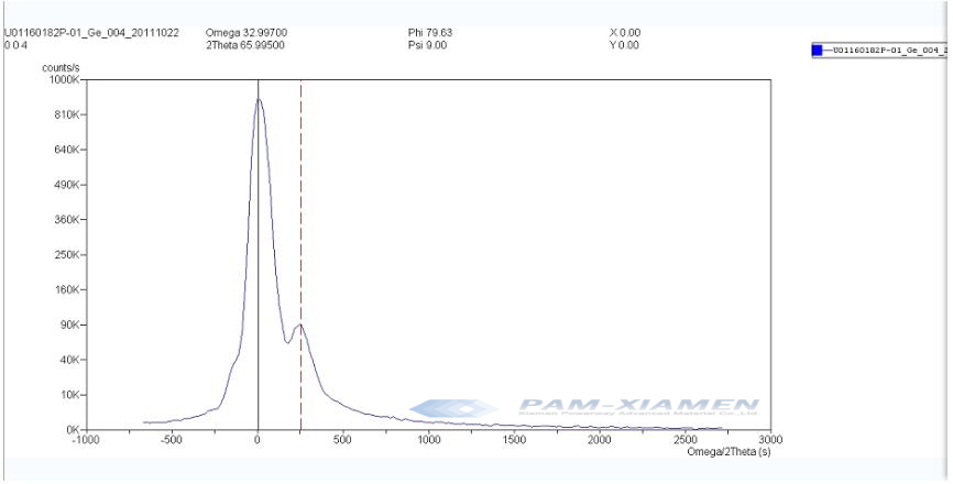
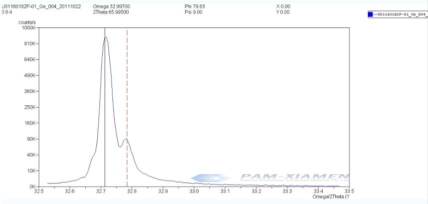
PAM XIAMEN offers 4″ Silicon Wafer.
Material
Orient.
Diam.
Thck
(μm)
Surf.
Resistivity
Ωcm
Comment
p-type Si:B
[110] ±0.5°
4″
500
P/E
FZ >10,000
Prime, TTV<5μm
p-type Si:B
[110] ±0.5°
4″
200
P/P
FZ 1-2
SEMI Prime
p-type Si:B
[110] ±0.5°
4″
200
P/P
FZ 1-2
Prime
p-type Si:B
[110] ±0.5°
4″
200
P/P
FZ 1-2
SEMI Prime, Extra 8 scratched wafers in cassette free of charge
p-type Si:B
[100]
4″
220 ±10
P/E
FZ >10,000
SEMI Prime
p-type Si:B
[100]
4″
230 ±10
P/E
FZ >10,000
SEMI Prime
p-type Si:B
[100-4° towards[110]] ±0.5°
4″
525
P/E
FZ >2,000
SEMI Prime, TTV<5μm
p-type Si:B
[100]
4″
450
P/P
FZ 1,000-2,000
SEMI Prime
p-type Si:B
[100]
4″
420
C/C
FZ 850-900
SEMI Prime
p-type Si:B
[100]
4″
200 ±10
P/P
FZ 100-120
SEMI Prime
p-type Si:B
[100]
4″
250
P/P
FZ 1-3 {0.97-1.01}
SEMI [...]
2019-03-05meta-author
PAM-XIAMEN can offer 4 inch test grade silicon wafer with single side polished. The parameters for 4″-SSP Si wafer at test grade are as follows:
1. Parameters of Si Single Crystal Wafer at Test Grade
PAM-210310-Si wafer
Sl No
Item
Specifications
1
Growing Method
CZ
2
Wafer Diameter
100±0.5 mm
3
Wafer Thickness
525±25 μm
4
Wafer Surface Orientation
<100>±0.5º
5
Type
P type
6
Dopant
Boron
7
Dislocation Density
Less than 5000/cm2
8
Resistivity
2-8 [...]
2021-04-14meta-author
PAM XIAMEN offers 1″ silicon wafers.
If you don’t see what you need, pleaes email us your specs and quantity.
Item
Dia
Thickness (um)
Orientation
Type
Dopant
Resistivity
(Ohm-cm)
Polish
Remark
PAM1901
25.4mm
20000um
<111>
P
B
>1000
DSP
FZ
PAM1902
25.4mm
400um
<100>
P
B
ANY
SSP
Thickness is: 400+/-100um.
PAM1903
25.4mm
500um
<100>
ANY
SSP
Wafers have particles. Wafers sold “As-Is”.
PAM1904
25.4mm
280um
<111>
Undoped
Undoped
>2000
SSP
Intrinsic FZ
PAM1905
25.4mm
73.5um
<100>
Undoped
Undoped
>5000
DSP
FZ, Float Zone
PAM1906
25.4mm
500um
<100>
P
B
.01-.05
DSP
NO flats, COMPLETELY round. Minimum Order Quantity 5 wafers.
Item
Material
Orient.
Diam
(mm)
Thck
(μm)
Surf.
Resistivity
Ωcm
Comment
PAM1907
p-type Si:B
[100]
1″
280um
P/E
0-100 ohm-cm
SEMI, 1Flat, Soft cst
PAM1908
Intrinsic Si:-
[111]
1″
280um
P/E
FZ [...]
2019-02-21meta-author
PAM-XIAMEN offers GaN on silicon HEMT wafer for Power, E-mode. Because the normally-on characteristic will Increase the complexity of circuit design and power consumption, designing an enhanced (E-Mode) HEMT that is turned off under zero grid bias will be crucial for advancing the application of GaN-on-Silicon HEMT in [...]
2019-05-17meta-author
A Glance of GaAs Wafer Market
According to Mamms Consulting, as one of the most mature compound semiconductors, GaAs is everywhere, and it has become the cornerstone of power amplifiers in every smart phone! In 2018, the GaAs RF business is expected to account for [...]
2018-09-05meta-author
GaAs epi wafer for microelectronic and optoelectronic devices
PAM XIAMEN offers GaAs epi wafer for microelectronic and optoelectronic devices including MESFET HEMT, ICMMIC HBT, HALL device, visible light LED, IR LED, LD and solar cell.
Electronic devices
Material(layer/substrate)
Application
Technology Tends
Material Required
Digital IC
(MESFETHEMT)
GaAs/GaAs
GaAlAs/GaAs
Ultra-high-speed computers
PC,ATM,Image Processing
High level [...]
2019-03-15meta-author