In solid state physics, a band gap, also called an energy gap or bandgap, is an energy range in a solid where no electron states can exist. In graphs of the electronic band structure of solids, the band gap generally refers to the energy difference (in electron volts) between the top of the valence band and the bottom of the conduction band in insulators and semiconductors shown as figure below. This is equivalent to the energy required to free an outer shell electron from its orbit about the nucleus to become a mobile charge carrier, able to move freely within the solid material. So the band gap is a major factor determining the electrical conductivity of a solid. Substances with large band gaps are generally insulators, those with smaller band gaps are semiconductors, while conductors either have very small band gaps or none, because the valence and conduction bands overlap. PAM-XIAMEN can supply single crystal wafers with direct or indirect band gap.
There are two types of band gaps, direct and indirect due to the different transition methods:
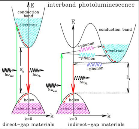
Schematic of Direct Band Gap and Indirect Band Gap
1. Vertical Transition (Direct Light Absorption Process)
Corresponding to the case where the bottom of the conduction band and the top of the valence band are at the same point in k-space. In this transition, the wave vector of the electron can be regarded as constant. This is a vertical transition, and we call this semiconductor a direct bandgap semiconductor. Among all semiconductors, the GaAs, InP, InSb, etc are direct band gap semiconductors.
Important properties of direct bandgap semiconductors: When the electrons in the valence band transition to the conduction band, the wave vector of the electrons remain unchanged, this is a vertical transition on the energy band diagram. This means that the momentum of the electron can remain unchanged during the transition process, satisfying the law of conservation of momentum.
Conversely, if the conduction band electrons fall to the valence band (that is, electrons recombine with holes), they can also keep their momentum unchanged—direct recombination, that is, recombination occurs as soon as electrons and holes meet (no phonons are required to accept or provide momentum). Therefore, the lifetime of carriers in direct bandgap semiconductors will be very short; at the same time, this direct recombination can release almost all energy in the form of light, so luminous efficiency is very high. That’s why most light-emitting devices are made of direct bandgap semiconductors.
2. Non-Vertical Transition (Indirect Light Absorption Process)
Corresponding to the case where the conduction band edge and the valence band edge are at different points in the K space. Simply absorbing a photon transitions from the top of the valence band to the bottom of the conduction band, and the electron absorbs the photon and simultaneously absorbs or emits a phonon. Semiconductors whose conduction and valence band edges are at different points in k-space are often referred to as indirect bandgap semiconductors. Forming a half-full band requires not only absorbing energy, but also changing momentum. We call this the indirect band gap. Therein, indirect bandgap semiconductors include Ge, Si, etc. The non-vertical transition that occurs in indirect band gap semiconductors is a second-order process that occurs much less often than vertical transitions
It can be seen from the energy band map that the K value of the electrons in the indirect band gap semiconductor will change during the transition. This means that the positions of the electrons in the K space before and after the transition are different, so there is a great probability of releasing energy to the lattice, converting it into phonons, and releasing it as heat energy. However, the electrons in the direct band gap only have energy changes before and after the transition, but no position changes, so there is a greater probability of releasing energy in the form of photons. On the other hand, for the indirect transition type, electrons in the conduction band need momentum to recombine with holes in the valence band. Therefore, it is difficult to generate luminescence based on recombination. If you want the indirect bandgap material to emit light, doping can be introduced into the light-emitting body to improve the luminous efficiency.

For more information, please contact us email at victorchan@powerwaywafer.com and powerwaymaterial@gmail.com.