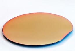
PAM-XIAMEN offers 1550nm laser diode wafer, which is an epitaxial wafer of a diode laser structure emitting around 1550 nm (on InP substrate), and the wafer dimension for laser diode 1550nm can be 2” or 3”. You can fabricate a laser for your application such as output cw power around 10-20 mW. Following are InP-based GaAs epitaxial wafers, which involve a multiple quantum well which has an optical response at the wavelength 1.55um (usually, MQW of InGaAsP\InAsP\InP) for modulators @1.55um and high-speed modulator in the telecom\datacome industry..

1. Structures of 1550nm Laser Diode Wafer
Structure1:
| Layer | Material | Thickness(nm) | Carrier Concentratin (cm-3) |
Type | Dopant |
| Contactlayer | In0.53GaAs | — | — | P | — |
| Ohmiccontact | 1.52Q InGaAsP |
— | — | P | Zn |
| Ohmiccontact | 1.3Q InGaAsP |
— | — | P | — |
| Cladding | InP | — | — | P | Zn |
| Etchstop | 1.1Q InGaAsP |
— | — | P | — |
| Spacer | InP | — | — | P | Zn |
| SubCladding | AlInAs | — | — | — | — |
| GRIN-SCH | [AlxGa]InyAs | — | — | — | — |
| QB | [AlxGa]InyAs | — | — | — | — |
| QW | [AlxGa]InyAs | — | — | — | — |
| GRIN-SCH | [AlxGa]InyAs | — | — | — | — |
| Sub Cladding | [[AlxGa]InyAs | — | — | — | — |
| Graded layer | [[AlxGa]InyAs | — | — | N | Si |
| Cladding | InP | — | — | N | Si |
| Buffer | InP | — | — | — | Si |
| Substrate | InP Substrate | ||||
Structure2: PAM-200604-LD-1550
| Layer | Material | Thickness(nm) | Carrier Concentration(cm-3) | Dopant | Type |
| 6 | InP | 20 | — | Zinc | P |
| 5 | GaIn(x)As | — | — | Zinc | P |
| 4 | GaIn(x)As(v)P | — | — | Zinc | P |
| 3 | InP | 2300 | — | Zinc | P |
| 2 | AlGaInAs MQW | — | — | Undoped | U/D |
| PL 1500~1560nm | — | — | — | — | |
| 1 | InP buffer | — | — | silicon | N |
| InP substrate | — | — | — | — |
2. Development and Application of 1550nm Laser Diode Wafer
In recent years, optical communication technology has achieved unprecedented vigorous development all over the world. Therefore, the research of lasers as the most widely used core component of the optical emission part has aroused people’s great interest. InGaAsP material is an important material for the production of optoelectronic and microwave devices. The laser made of InGaAsP material can continuously change its emission wavelengths in the range of 1.1um to 1.65um, and this range covers the wavelength of 1.3um and 1.55um of quartz fiber, which are the windows of low dispersion and low loss.
As new infrastructure drives the development of 5G and data centers, smartphones use 3D sensing technology and the continuous development of industrial laser processing, laser medical treatment, lidar and other applications. As a key material for lasers and detector chips, GaAs/InP-based optoelectronic epitaxial wafers are in short supply. 1550nm laser diode fabricated on GaAs/InP-based wafer is prepared by industry chain technology and packaging companies. 1550nm laser diode wafers are widely used in industrial fields such as optical fiber communication, laser sensing, and consumer electronics fields such as smart phones and AR/VR.
3. FAQ of Laser Diode Wafer
Q:Actually, I aminterested to know about epitaxial growth of InP to make laser at 1550 nm. I appreciate if you could comment on that based on your experience, and give me a comment on the output power of laser.
A:The lasers fabricated on PAM-200604 InP based 1550nm laser diode wafer has following electrical characteristics:
Output power: 3W
Input power:11.2W
@100um stripe width, 7A, 1.2V. (190306)
For more information, please contact us email at victorchan@powerwaywafer.com and powerwaymaterial@gmail.com

