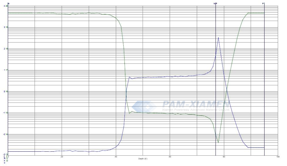
PAM XIAMEN offers GaN SBD.
Parmeters
Specification
BV
300~650
If
1~20
Operation temp.
-55~150
Trr
<10
Package type
TO220-2L
TO220-3L
For more information, please visit our website: https://www.powerwaywafer.com,
send us email at sales@powerwaywafer.com and powerwaymaterial@gmail.com
Found in 1990, Xiamen Powerway Advanced Material Co., Ltd (PAM-XIAMEN) is a leading manufacturer of semiconductor material in China. PAM-XIAMEN develops advanced crystal [...]
2019-05-17meta-author
PAM-XIAMEN, a leading SiC epitaxial wafer manufacturer, can offer 4H SiC epitaxial wafers for MOS fabrication, which refer to a single crystal film(epitaxial layer) with certain requirements and the same crystal growing on a silicon carbide substrate. The SiC epitaxial wafer market size is [...]
2021-05-17meta-author
PAM-XIAMEN offers 850nm laser diode wafer, which is a SLD (superluminescent diode) structure. It can be used as the light source of fiber optic gyroscope. Super-luminescent diode is a kind of semiconductor optoelectronic devices between laser diodes (LDs) and light-emitting diodes (LEDs). More detail [...]
2019-03-13meta-author
PAM XIAMEN offers 60+1mm FZ Si Ingot -2
FZ Si Ingot
Diameter 60+1mm, N-type, <111>±2°
Resistivity>3000Ωcm
Oxygen/Carbon Content 10Е16см-3
The silicon content not less than 99.999999%
Length 150-480mm
MCC lifetime>1000μs
The dislocation density not, Swirl not
For more information, send us email at sales@powerwaywafer.com and powerwaymaterial@gmail.com
2020-03-11meta-author
X-ray diffraction analysis of LT-GaAs multilayer structures
Multilayer structures of low-temperature-grown GaAs(LT-GaAs) into which ultra-thin layers containing excess As are periodically introduced are grown by molecular beam epitaxy. The concentration of excess As in the ultra-thin layers is determined by the analysis of the intensity [...]
PAM XIAMEN offers Yb YAG Ytterbium (Yb) doped Yttrium Aluminium Garnet Laser Crystal.
Ytterbium – Yb:YAG is a very promising laser crystal and is more suitable for diode-pumping than the commonly used Nd-doped YAG crystals. Compared with the traditional Nd:YAG crystal, Yb:YAG crystal has a much wider [...]
2019-03-15meta-author

