4H N type SiC wafer with Nitrogen doped is available, size from 2” to 4”. Dummy wafer and prime wafer are available. High quality single crystal SiC wafer are available for MBE growth research, electronics and optoelectronics industries. SiC wafer is a next-generation semiconductor material with unique electrical properties and excellent thermal properties. Compared with silicon wafer and GaAs wafer, n doped silicon carbide wafer is more suitable for high temperature and high power devices.
1. Specifications of 4H N Type SiC Wafer
1.1 4H N-TYPE SIC, 2″WAFER SPECIFICATION
| SUBSTRATE PROPERTY | S4H-51-N-PWAM-250 S4H-51-N-PWAM-330 S4H-51-N-PWAM-430 |
| Description | A/B Production Grade C/D Research Grade D Dummy Grade 4H SiC Substrate |
| Polytype | 4H |
| Diameter | (50.8 ± 0.38) mm |
| Thickness | (250 ± 25) μm (330 ± 25) μm (430 ± 25) μm |
| Carrier Type | n-type |
| Dopant | Nitrogen |
| Resistivity (RT) | A/B:0.012 – 0.028 Ω·cm;C:0.012 – 0.1 Ω·cm;D:0.02 – 0.3 Ω·cm |
| Surface Roughness | < 0.5 nm (Si-face CMP Epi-ready); <1 nm (C- face Optical polish) |
| FWHM | A<30 arcsec B/C/D <50 arcsec |
| Micropipe Density | A+≤1cm-2 A≤10cm-2 B≤30cm-2 C≤50cm-2 D≤100cm-2 |
| Surface Orientation | |
| On axis | <0001>± 0.5° |
| Off axis | 4°or 8° toward <11-20>± 0.5° |
| Primary flat orientation | Parallel {1-100} ± 5° |
| Primary flat length | (16 ± 1.7) mm |
| Secondary flat orientation | Si-face:90° cw. from orientation flat ± 5° |
| C-face:90° ccw. from orientation flat ± 5° | |
| Secondary flat length | (8 ± 1.7) mm |
| Surface Finish | Single or double face polished |
| Packaging | Single wafer box or multi wafer box |
| Usable area | A:≥ 90 %;B:≥ 85 %;C:≥ 80 %;D:≥ 70 % |
| Edge exclusion | 1 mm |
1.2 4H-SIC Wafer, N-TYPE , 3″WAFER SPECIFICATION
| SUBSTRATE PROPERTY | S4H-76-N-PWAM-330 S4H-76-N-PWAM-430 |
| Description | A/B Production Grade C/D Research Grade D Dummy Grade 4H SiC Substrate |
| Polytype | 4H |
| Diameter | (76.2 ± 0.38) mm |
| Thickness | (350 ± 25) μm (430 ± 25) μm |
| Carrier Type | n-type |
| Dopant | Nitrogen |
| Resistivity (RT) | 0.015 – 0.028Ω·cm |
| Surface Roughness | < 0.5 nm (Si-face CMP Epi-ready); <1 nm (C- face Optical polish) |
| FWHM | A<30 arcsec B/C/D <50 arcsec |
| Micropipe Density | A+≤1cm-2 A≤10cm-2 B≤30cm-2 C≤50cm-2 D≤100cm-2 |
| TTV/Bow /Warp | <25μm |
| Surface Orientation | |
| On axis | <0001>± 0.5° |
| Off axis | 4°or 8° toward <11-20>± 0.5° |
| Primary flat orientation | <11-20>±5.0° |
| Primary flat length | 22.22 mm±3.17mm 0.875″±0.125″ |
| Secondary flat orientation | Si-face:90° cw. from orientation flat ± 5° |
| C-face:90° ccw. from orientation flat ± 5° | |
| Secondary flat length | 11.00 ± 1.70 mm |
| Surface Finish | Single or double face polished |
| Packaging | Single wafer box or multi wafer box |
| Scratch | None |
| Usable area | ≥ 90 % |
| Edge exclusion | 2mm |
1.3 4H N TYPE SIC 4″ WAFER SPECIFICATION
| SUBSTRATE PROPERTY | S4H-76-N-PWAM-330 S4H-76-N-PWAM-430 |
| Description | A/B Production Grade C/D Research Grade D Dummy Grade 4H SiCSubstrate |
| Polytype | 4H |
| Diameter | (76.2 ± 0.38) mm |
| Thickness | (350 ± 25) μm (430 ± 25) μm |
| Carrier Type | n-type |
| Dopant | Nitrogen |
| Resistivity (RT) | 0.015 – 0.028Ω·cm |
| Surface Roughness | < 0.5 nm (Si-face CMP Epi-ready); <1 nm (C- face Optical polish) |
| FWHM | A<30 arcsec B/C/D <50 arcsec |
| Micropipe Density | A+≤1cm-2 A≤10cm-2 B≤30cm-2 C≤50cm-2 D≤100cm-2 |
| TTV/Bow /Warp | <45μm |
| Surface Orientation | |
| On axis | <0001>± 0.5° |
| Off axis | 4°or 8° toward <11-20>± 0.5° |
| Primary flat orientation | <11-20>±5.0° |
| Primary flat length | 32.50 mm±2.00mm |
| Secondary flat orientation | Si-face:90° cw. from orientation flat ± 5° |
| C-face:90° ccw. from orientation flat ± 5° | |
| Secondary flat length | 18.00 ± 2.00 mm |
| Surface Finish | Single or double face polished |
| Packaging | Single wafer box or multi wafer box |
| Scratch | None |
| Usable area | ≥ 90 % |
| Edge exclusion | 2mm |
PAM-XIAMEN also can offer the following specifications:
4H N type SiC Substrate,5mm*5mm, 10mm*10mm WAFER SPECIFICATION : Thickness:330μm/430μm
4H N-type SiC Thin Film,15mm*15mm, 20mm*20mm WAFER SPECIFICATION: Thickness:330μm/430μm
a-plane SiC Wafer, size: 40mm*10mm,30mm*10mm,20mm*10mm,10mm*10mm,specs below:
4H N type SiC Wafer Thickness:330μm/430μm or custom
2. About 4H-SiC Properties
2.1 4H-SiC Properties VS. 6H-SiC Properties
| Polytype | Single Crystal 4H | Single Crystal 6H |
| Lattice Parameters | a=3.076 Å | a=3.073 Å |
| c=10.053 Å | c=15.117 Å | |
| Stacking Sequence | ABCB | ABCACB |
| Band-gap | 3.26 eV | 3.03 eV |
| Density | 3.21 · 103 kg/m3 | 3.21 · 103 kg/m3 |
| Therm. Expansion Coefficient | 4-5×10⁻⁶/K | 4-5×10⁻⁶/K |
| Refraction Index | no = 2.719 | no = 2.707 |
| ne = 2.777 | ne = 2.755 | |
| Dielectric Constant | 9.6 | 9.66 |
| Thermal Conductivity | 490 W/mK | 490 W/mK |
| Break-Down Electrical Field | 2-4 · 108 V/m | 2-4 · 108 V/m |
| Saturation Drift Velocity | 2.0 · 105 m/s | 2.0 · 105 m/s |
| Electron Mobility | 800 cm2/V·S | 400 cm2/V·S |
| hole Mobility | 115 cm2/V·S | 90 cm2/V·S |
| Mohs Hardness | ~9 | ~9 |
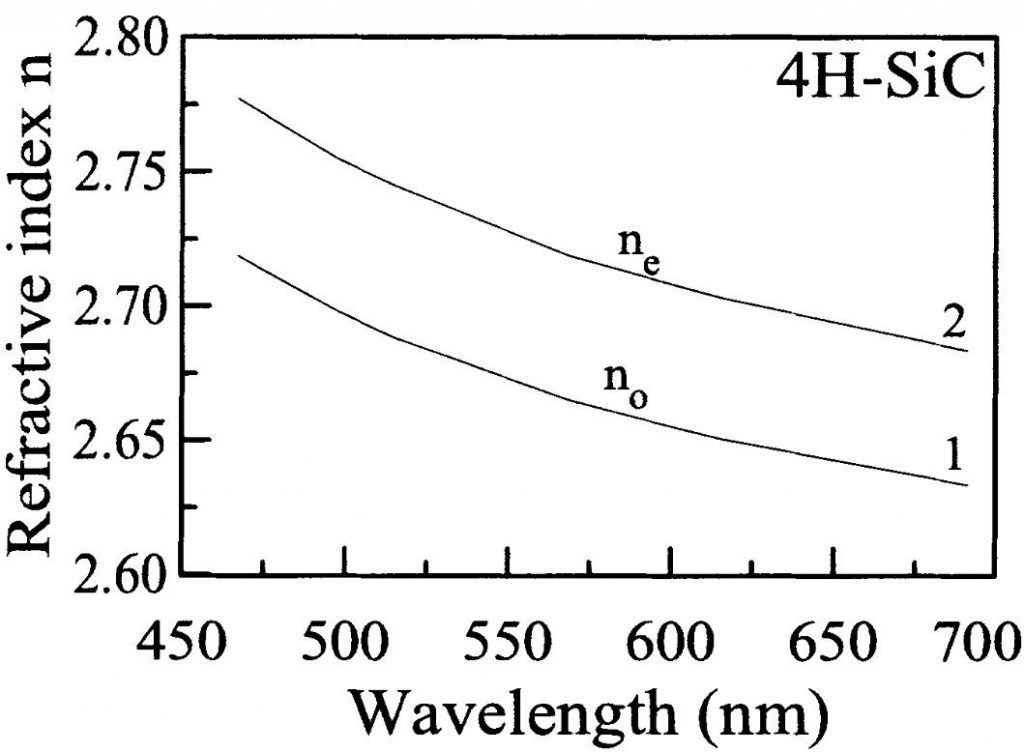
2.2 Optical Property of 4H N Type SiC Wafer
4H SiC refractive index decreases with the increasing of wavelength:
The 4H SiC bandgap is declining when the temperature goes up:

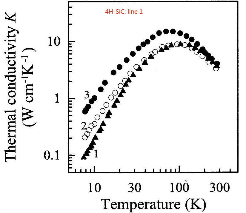
2.3 4H SiC Substarte Thermal Property
4H SiC thermal conductivity is changing along with the temperature. When the temperature is low(about 40℃), the the thermal conductivity of 4H N type SiC wafer is climbing up; however, when the temperature is high over 40℃, it begins down slowly:

For more information, please contact us email at victorchan@powerwaywafer.com and powerwaymaterial@gmail.com.