PAM-XIAMEN offers 650V GaN FETs chip for fast charge. In current market, gallium nitride fast charging sources mainly use 650V GaN chip (GaN FETs) as power switches, and the high-frequency characteristics of gallium nitride are used to make terminal fast charging products smaller in size and higher in efficiency.
The PAM65D150DNBI-TS series 650V, 150mΩ gallium nitride(GaN) FETs are normally-on devices. PAM-XIAMEN GaN chip offers better efficiency through lower gate charge, faster switching speeds, and smaller reverse recovery charge, delivering significant advantages over traditional silicon(Si) devices. PAM-XIAMEN is one of leading-edge GaN chip makers with world-class innovation.
1. Parameters of 650V GaN FETs Chip
| Symbol | Parameter | Limit value | Unit |
| RθJC | Junction-to-case | 1.3 | °C /W |
1.1 Absolute Maximum Ratings of 650V GaN FETs Chip (TC=25°C unless otherwise stated)
| Symbol | Parameter | Limit value | Unit | |
| VDSS | Drain to source voltage | 650 | V | |
| VDSS | Gate to source voltage | 一25~+2 | ||
| ID | Continuous drain current @TC=25°C | 15 | A | |
| Continuous drain current @TC=100°C | 10 | |||
| IDM | Pulse drain current | 65 | A | |
| PD | Maximum power dissipation @ TC=25°C | 65 | W | |
| TC | Operating temperature | Case | 一55~150 | °C |
| TJ | Junction | 一55~175 | °C | |
| TS | Storage temperature | 一55~150 | °C | |
Top Bottom
1.2 Electrical Parameters of 650V GaN Chipset (TJ=25°C unless otherwise stated)
| Symbol | Parameter | Min | Typ | Max | Unit | Test Conditions |
| Forward Device Characteristics | ||||||
| V(BL)DSs | Drain-source voltage | — | 650 | — | v | Vcs=-25V |
| Vasth) | Gate threshold voltage | — | -18 | — | v | VDs=Vas,IDs=luA |
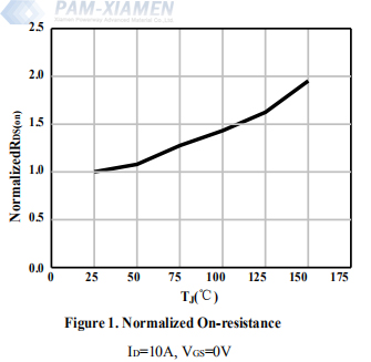
| RDS(on) | Drain-source on-resistance | — | 150 | 180 | mQ | Vcs=OV,ID-10A |
| — | — | — | VGs=OV, ID-10A,TJ=150’C | |||
| lDss | Drain-to-source leakage current |
— | — | 3 | uA | VDs=650V,VGs=-25V |
| — | — | 30 | VDs=400V,VGs=-25V, T=150’c |
|||
| lass | Gate-to-source forward leakage current |
— | 3.7 | 100 | nA | VGs=2V |
| Gate-to-source reverse leakage current |
— | -3.5 | -100 | VGS=-25V | ||
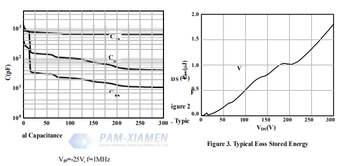
| CIss | Input capacitance | — | 650 | — | pF | vGs=-25V,VDS=300V,f=1MHz |
| Coss | Output capacitance | — | 40 | — | ||
| CRSS | Reverse capacitance | — | 10 | — | ||
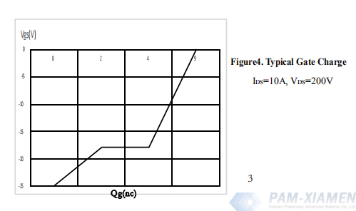
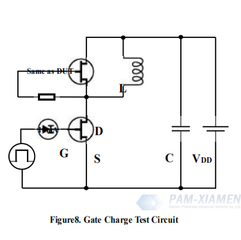
| QG | Total gate charge | — | 9 | — | nC | VDS=200V,VGS=-25V to ov, ID=10A |
| QGS | Gate-source charge | — | 2 | — | ||
| QGD | Gate-drain charge | — | 7 | — | ||
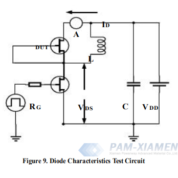
| tn | Reverse recovery time | — | 4 | — | ns | Is=0A to 11A,VDD=400V di/dt=1000A/uS |
| Q. | Reverse recovery charge | — | 17 | — | nC | — |
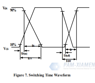
| TIX(on) | Turn-on delay | — | 0.5 | — | — | VDs=200VVG=-25V to ov, ID=10A |
| tR | Rise time | — | 9 | — | ||
| tD(off) | Turn-off delay | — | 0.5 | — | ||
| tF | Fall time | — | 10 | — | ||
| Reverse Device Charactcristics | ||||||
| VSD | Reverse voltage | — | 7 | — | v | VGS=-25V,Is=10A,Tc=25′ C |
1.3 Typical Characteristics of 650V GaN Charger Chip (TJ=25°C unless otherwise stated)
1.4 Test Circuit and Waveforms of 650V GaN Power Chip

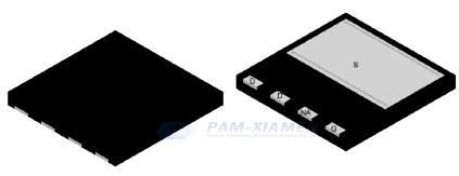
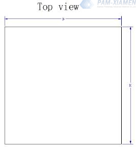
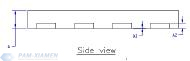
1.5 PACKAGE DIMENSIONS of 650V GaN Chip
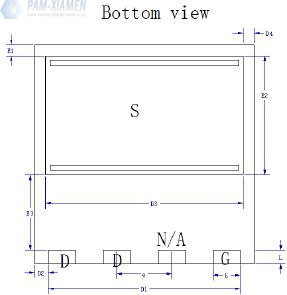
| ITEM | I.ow 1imit (mm) |
Center (mm) |
Upper 1imit (mm) |
| A | 0.80 | — | 1.00 |
| A1 | 0 | — | 0.05 |
| A2 | 0.15 | 0.25 | 0.35 |
| b | 0.9 | 1 | 1.1 |
| D | 7.9 | 8 | 8.1 |
| D1 | 6.9 | 7 | 7.1 |
| D2 | 0.4 | 0.5 | 0.6 |
| D3 | 7.1 | 7.2 | 7.3 |
| D4 | 0.3 | 0.4 | 0.5 |
| E | 7.9 | 8 | 8.1 |
| E1 | 0.3 | 0.4 | 0.5 |
| E2 | 4.25 | 4.35 | 4.45 |
| E3 | 2.65 | 2.75 | 2.85 |
| e | 1.9 | — | 2.1 |
| L | 0.4 | 0.5 | 0.6 |
2. General Features of 650V GaN Power FETs
Easy to drive—compatible with standard gate drivers
Low conduction and switching losses
Low Qrr of 17nC—no free-wheeling diode
required
RoHS compliant and Halogen-free
3. Automotive of 650V GaN FETs Chip
Fast charger
Renewable energy
Telecom and data-com
Servo motors
Industrial
Automotive
4. Benefits of 650V GaN Chip
Increased efficiency through fast switching
Increased power density
Reduced system size and weight
As a representative of the third generation of semiconductor materials, when gallium nitride is used in fast charging devices, the output power of GaN chip devices is three times that of traditional materials in the case of the same size. GaN FET technology is redefining the standard for fast charging of mobile phones. The third-generation semiconductor industry is also ushering in new developments due to the application of gallium nitride.

For more information, please contact us email at victorchan@powerwaywafer.com and powerwaymaterial@gmail.com