You can buy single crystal AlN substrate with higher photoelectric conversion efficiency than indirect band gap semiconductors from PAM-XIAMEN. Aluminum nitride (AlN) is an important blue and ultraviolet light-emitting material, which is used in ultraviolet/deep ultraviolet light-emitting diodes, ultraviolet laser diodes, and ultraviolet detectors. In addition, AlN can form a continuous solid solution with III nitrides such as GaN and InN, and its ternary or quaternary alloy can achieve continuous adjustment of its band gap from the visible band to the deep ultraviolet band, making it an important high-performance luminescence material. Here are the specifications we offered:
1. Single Crystal AlN Substrate Wafer
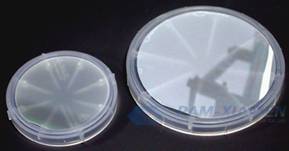
PAM210702-AS
| Diameter | 10 mm* | |
| Thickness | 400 ± 50 µm | |
| Crystal type | 2H | |
| Orientation | {0001}± 0.5° | |
| Surface Finish Al face | CMP(double side polishing is customizable) | |
| Roughness | Al face | ≤0.5 nm |
| N face (backside) | ≤1.2 µm | |
| Shape | Round | |
| Scratches | None | |
| Chips | None | |
| XRD@(0002) | ≤300 arcsec | |
| Absorption Coefficient | ≤100 cm-1 | |
| Usable Area | ≥90% | |
| TTV | ≤30 µm | |
| Bow | ≤30 µm | |
| Wrap | ≤30 µm | |
| Cracks | None, by naked eye, high intensity light | |
| Surface Contamination | None, by naked eye, diffuse light | |
| Packaging | Single wafer cups | |
The following sizes are available:
| Sl. No. | Size |
| PAM-AIN-01010 | 10x10mm |
| PAM-AIN-010 | Dia. 10mm |
| PAM-AIN-015 | Dia. 15mm |
| PAM-AIN-020 | Dia. 20mm |
| PAM-AlN-025 | Dia. 25.4mm |
| PAM-AIN-030 | Dia. 30mm |
| PAM-AIN-050 | Dia. 50.8mm |
| PAM-AIN-M | M-plane |
2. Advantages and Disadvantages of AlN Substrate Growth Process
At present, although the AlN single crystal substrate prepared by the PVT method has been commercialized; the AlN substrate price is very high, which hinders its large-scale commercialization. In addition, the AlN single crystal grown by the PVT method is usually yellow or brown, and has poor light transmittance, which is not conducive to the preparation of deep ultraviolet light-emitting devices as a substrate. Therefore, in order to realize the large-scale application of transparent single crystal AlN substrate, it is necessary to propose an efficient and low-cost preparation scheme.
In the prior art, common growth processes for preparing single crystal AlN include metal organic chemical vapor deposition (MOCVD), physical vapor transport (PVT) and hydride vapor phase epitaxy (HVPE). The advantages and disadvantages of these three processes are as follows:
The advantages of the MOCVD process are: a large area of AlN thin film crystal material can be prepared, the area of which is determined by the size of the growth chamber, and the maximum diameter is 6 inches; it can be prepared to obtain various fine structures and have a very flat surface. It is related to the slower growth rate of the material under the MOCVD process.
However, the disadvantages of the MOCVD process are: it is difficult to overcome the stress and high dislocations caused by heteroepitaxial; and the material growth rate of the MOCVD process is slow (a few hundred nanometers per hour), which is not suitable for preparing commercial AlN substrate with a thickness of hundreds of microns. The pre-reaction of the metal aluminum organic compound TMAl and NH 3 is serious.
The advantage of the HVPE process is that a large area of AlN single crystal material can be prepared. The area of the AlN single crystal material is determined by the size of the heterogeneous substrate and the growth chamber. At present, the largest area is only 2 inches in diameter. HVPE has a fast growth rate, can prepare AlN thick film single crystal materials (several hundred microns thick) used as a substrate, and has good heterogeneous threading dislocations (dislocation density 106cm-2-107cm-2).
However, the disadvantages of the HVPE process are: it is difficult to directly grow heteroepitaxially to obtain a material with a flat surface and high crystallinity; it is difficult to overcome the bending and cracking of the epitaxial film caused by the stress caused by the heteroepitaxial growth, which makes it difficult to obtain a heterogeneous lining. Stripping from the bottom to obtain a complete, large-area unsupported AlN thick film single crystal material, the material yield is low, and it is not suitable for commercialization.
The advantages of PVT are: fast material growth (several hundreds of micrometers per hour); low dislocation density (102cm-2-104cm-2); low equipment maintenance costs; it is very easy to scale production when the process is mature.
However, the disadvantages of the PVT process are: the material growth temperature is very high, and there is a high requirement for the temperature gradient control of the growth chamber; the AlN single crystals grown by PVT are mostly orange and brown, and the light transmission is not good; the polarity of the material is difficult control.
3. Technical Problems for Preparing Single Crystal AlN Wafer
To make the AlN commercialized, AlN substrate manufacturers should take actions to solve the following technical problems:
Firstly, the UV light absorption problem of AlN single crystal substrate prepared by PVT is still not solved. Therefore, after obtaining HVPE-AlN single crystal, in order to improve the luminescence performance of deep ultraviolet light-emitting devices, chemical mechanical polishing (CMP) method to remove the poorly transparent PVT-AlN substrate and this PVT-AlN substrate is a high-quality single crystal AlN material, which is extremely expensive. Therefore, the substrate material is ground to obtain the AlN single crystal. This is a great waste, and the production cost of deep ultraviolet light-emitting devices is increased;
Secondly, the CMP process itself is time-consuming and labor-intensive, and the surface of the processed material is uneven, which is prone to oxidation problems;
Thirdly, the AlN grown by the HVPE process has a lot of stress, and problems such as cracks are prone to occur during the grinding and polishing process.
4. AlN Single Crystal Substrate Application
AlN crystal is an ideal substrate for GaN, AlGaN and AlN epitaxial materials. Compared with sapphire or SiC substrates, AlN and GaN have higher thermal matching and chemical compatibility, and the stress between the substrate and the epitaxial layer is smaller. Therefore, when AlN crystal is used as a substrate for epitaxial growth of GaN, it can greatly reduce the defect density in the device, improve the performance of the device, and have a good application prospect in the preparation of high-temperature, high-frequency, and high-power electronic devices.
In addition, using AlN substrate to grow high aluminum (Al) component AlGaN epitaxial material can also effectively reduce the defect density in the nitride epitaxial layer, and greatly improve the performance and service life of nitride semiconductor devices. In addition, AlN substrate wafer has a high nonlinear optical coefficient and can be used in second harmonic transmitters.

For more information, please contact us email at victorchan@powerwaywafer.com and powerwaymaterial@gmail.com.