High transparency AlN template on sapphire and silicon substrate are available from PAM-XIAMEN, which are suitable for making high-frequency BAW, SAW devices and power electronic. Aluminum nitride (AIN) template not only has the characteristics of AIN piezoelectric film, but also has the characteristics of higher sound propagation rate, lower sound loss, larger electromechanical coupling coefficient and thermal expansion coefficient similar to Si. Therefore, it has broad application prospects in the fields of surface acoustic wave (SAW) and bulk acoustic wave (BAW) device and high-frequency broadband communications. Because the AIN film has high BAW speed (11300m/s) and SAW speed (>7500m/s), the BAW and SAW fabricated on epiready AlN template have obvious advantages.
1. Single Crystal AlN Specifications
AlN Crystal Substrate(PAM210702-AlN)
| Size | 10 x 10 mm | |
| Thickness | 400 ± 50 µm | |
| Crystal type | 2H | |
| Orientation | {0001}± 0.5° | |
| Surface Finish Al face | CMP,single side polished | |
| Roughness | Al face | ≤0.5 nm |
| N face (backside) | ≤1.2 µm | |
| Shape | Rectangle | |
| Scratches | None | |
| Cumulative Length | ≤1.0 mm | |
| Usable Area | ≥90% | |
| TTV | ≤ 30 µm | |
| Bow | ≤ 30 µm | |
| Wrap | ≤ 30 µm | |
| Cracks | None ,by naked eye ,high intensity light | |
| Surface Contamination | None, by naked eye, diffuse light | |
| Packaging | Single wafer cups | |
0.04” Thick Graphite Substrate for RTP Furnace’s Sample Holder, 3” or 5” O.D Selectable – EQ-G-Holder
3” Dia x 0.025” Thick Aluminum Nitride Substrate for RTP Furnace’s Sample Holder – EQ-AIN-Holder
AlN Single crystal
AlN Single Crystal Substrate <0001>,10x10x0.45mm, 2SP
AlN Single Crystal Substrate <0001>,5x5x0.45mm, 2SP
AlN Template on Silicon
Undoped AlN Template on Silicon ( Si <111> P type ) 5mmx5mm x 200 nm
Undoped AlN Template on Silicon ( Si <111> P type ) 10mmx10mm x 200 nm
AlN Template on 4″ Silicon ( Si <111>, P type, B-doped ) 4″x 500 nm
Undoped AlN Template on 2″ Silicon ( Si <111> N type ) 2″x 500 nm
Undoped AlN Template on 2″ Silicon ( Si <111> , N type ) 2″x 200 nm
Undoped AlN Template on 4″ Silicon ( Si, on <111> P type ) 4″x 200 nm
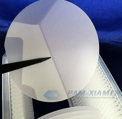
AlN Template on Sapphire
AlN Single Crystal Substrate <0001>,10x10x0.45mm, 2SP
AlN Single Crystal Substrate <0001>,5x5x0.45mm, 2SP
Undoped AlN Template on Sapphire, 2″x1000nm t- two sides polished
Undoped AlN Template on Sapphire 10x10mmx1000nm
Undoped AlN Template on Sapphire 10x10mmx5000nm
Undoped AlN Template on Sapphire 2″Dia. x1000nm thick,one side polished
Undoped AlN Template on Sapphire 5x5x0.5mm,1sp ,film: 1000nm
AlN Template on Sapphire, 2″x 5000 nm
AlN Template on Sapphire 4″x 1000 nm
AlN Template on Sapphire , 4″x 5000 nm
AlN templates, e.g. AlN epitaxial thin film on single crystal substrate, is the New Wave in Nitride Semiconductor Materials, which provides the most cost-effective solution to grow high quality III-V nitride thin film.
2. About Aluminum Ntride
AlN is the only stable phase in the AI-N binary system. It has a covalent bond and a hexagonal wurtzite structure and cannot melt under normal pressure, but decomposes at 2500K. Aluminum nitride has high optical transmittance in the entire visible and infrared frequency bands.
Here is a variety of excellent properties of AIN semiconductor material:
- The band gap is a a direct band gap of 6.2eV. So polycrystalline AlN layer is an important blue and ultraviolet light-emitting material;
- It has high thermal conductivity, high resistivity, strong breakdown field, low dielectric coefficient, which is excellent electronic materials with high temperature, high frequency and high power for devices;
- AIN oriented along the c-axis has very good piezoelectricity and high-speed propagation properties of surface acoustic waves, which is excellent Piezoelectric materials for surface acoustic wave devices;
- Aluminum nitride crystal and gallium nitride crystal have very close lattice constant and thermal expansion coefficient, which is the preferred substrate material for epitaxial growth of gallium nitride-based optoelectronic devices.
Comparison of AIN and other commonly used semiconductor materials in characteristics:
| Materials | AIN | Si | GaAs | GaN | 3C-SiC | 6H-SiC | SiO2 |
| Bandgap Width (eV) | 6.2 | 1.12 | 1.43 | 3.4 | 2.2 | 2.9 | 9 |
| Thermal Expansion Coefficient(10-6K-1) | 4.5 | 2.6 | 5.9 | 5.6 | 4.7 | 4.8 | 0.5 |
| Density(g/ cm3) | 3.26 | 2.33 | 5.32 | 6.09 | 3.20 | 3.20 | 2.27 |
| Breakdown Field Strength (106V/ cm) | 14 | 0.2 | 0.5 | >10 | 3 | 4 | 13 |
| Thermal Conductivity (W/cm℃) | 3.0 | 1.5 | 0.46 | 1.3 | 5 | 5 | 0. 014 |
| Dielectric Constant | 8.5 | 11.9 | 12.8 | 1 1.1 | 9.7 | 10 | 3.9 |
| Resistivity (ohm-cm) | >1013 | 1000 | 108 | >1010 | 150 | – | >1014 |
| Refractive Index | 2. 15 | 3.5 | 3.4 | 2.33 | 2.7 | 2.7 | 1.46 |
3. Epitaxial Growth of AlN
At present, the AlN growth technique is quite mature, and AIN thin films have been prepared by deposition using a variety of technologies. The most common methods include chemical vapor deposition (CVD), thermal evaporation, molecular beam epitaxy (MBE), pulsed laser deposition (PLD), ion beam nitridation, reactive magnetron sputtering (RS), and so on.
In addition to the growth technology of AlN epitaxial layer, another crucial factor in the epitaxial growth of thin films is the selection of a suitable substrate. Important items considered include crystal quality, lattice parameters, thermal expansion coefficient, practicality and price, etc. For the epitaxial growth of AlN template, the following table lists some commonly used substrate materials and parameters:
| Crystal Characteristics | AIN Hex. |
GaN Hex. |
InN Hex. |
a-Al2O3 Hex. |
6H-SiC Hex. |
Si
Cubic |
|
| Crystal Structure | |||||||
| Lattice Constant(A) | a | 3.111 | 3.186 | 3.545 | 4.758 | 3.081 | 5.43 |
| c | 4.979 | 5.178 | 5.703 | 11.991 | 15.092 | 5.43 | |
| c/a | 1.6 | 1.625 | 1.609 | 1.73 | 4.9 | 1 | |
| Thermal Expansion Coefficient | a | 4.2 | 5.59 | 5.7 | 7.5 | 4.2 | 3.59 |
| (10-6C-1) | c | 5.3 | 3.17 | 3.7 | 8.5 | 4.68 | 3.59 |
Among the substrates given in the table, Si has become the first substrate to be used because of its widely available characteristics, low cost, and mature technology. However, group II nitrides (AlN, GaN, and InN) have a large lattice mismatch with Si, their crystal structures (hexagonal wurtzite structure and cubic diamond structure) do not match, and the thermal expansion coefficients are also very different. This is why it is difficult to epitaxially grow AlN template on Si substrate, especially when thicker films need to be prepared.
The lattice parameters of 6H-SiC are relatively close to those of AlN (approximately within 1%), and have the same thermal expansion coefficient (4.2×10°C). Therefore, 6H-SiC is considered to be the preferred substrate for growing high-quality AlN template. However, compared with other substrates, due to the extremely high hardness of 6H-SiC, it is difficult to polish, resulting in particularly poor surface quality of 6H-SiC wafers. Poor surface topography of the substrate often results in poor film quality, and 6H-SiC is very expensive and not easy to obtain.
Sapphire (a-Al2O3) substrates have been successfully applied to the growth of sub-nitrides. Among nitrides, AlN has the closest performance correlation with sapphire. From a chemical point of view, the growth of AlN / sapphire template involves a simple conversion from Al oxide to nitride. It has been proved that AlN films are prepared by MOCVD or MBE. Due to the stability of sapphire and the shared c-axis hexagonal space group, (0001) oriented sapphire is suitable substrate for growing low-dislocation-density AlN templates.

For more information, please contact us email at victorchan@powerwaywafer.com and powerwaymaterial@gmail.com.