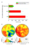


Silicon carbide (SiC) wafer material supplied by PAM-XIAMEN, like SiC substrate (link: https://www.powerwaywafer.com/sic-wafer/sic-wafer-substrate.html) is widely used in aerospace, radar communication, automotive industry and semiconductor industry due to its excellent properties such as high thermal conductivity, high strength, high temperature resistance and radiation resistance. However, [...]
PAM XIAMEN offers 6″FZ Prime Silicon Wafer-2 6″ Si wafer, Diameter 150mm, FZ Gas Dope, DSP, N(111), resistivity 5000-10,000Ωcm PARAMETER SPECIFICATION GENERAL CHARACTERISTICS 1 Growth Method FZ Gas Dope 2 Crystal Orientation (111) 3 Conductivity Type n 4 Dopant Phosphorus. 5 Nominal Edge Exclusion 6 mm ELECTRICAL CHARACTERISTICS 6 Resistivity 5000 – 10,000 Wcm 7 Life Time >1500 µsec CHEMICAL CHARACTERISTICS 8 Oxygen Concentrations < 2xE16 at/cm3 9 Carbon Concentrations < 2xE16 at/cm3 WAFER PREPARATION CHARACTERISTICS 10 Front Surface Condition Polished, DSP 11 Edge [...]
Xiamen Powerway Advanced Material Co.,Ltd., a leading supplier of AlGaP and other related products and services announced the new availability of size 2” is on mass production in 2017. This new product represents a natural addition to PAM-XIAMEN’s product line. Dr. Shaka, said, “We are [...]
PAM-XIAMEN offers larger size of N type FS GaN substrate including Si-doped and undoped one as follows: 1. N Type GaN Substrate Datasheet 1.1 4″(100mm) Undoped Free-standing GaN Substrate Item PAM-FS-GaN100-U Conduction Type Undoped Size 4″(100)+/-1mm Thickness 350-450um Orientation C-axis(0001)+/-0.5° Primary Flat Location (1-100)+/-0.5° Primary Flat Length – Secondary Flat Location (11-20)+/-3° Secondary Flat Length – Resistivity(300K) <0.5Ω·cm Dislocation Density <5×10^6cm-2 FWHM – TTV <=35um BOW <=50um Surface Finish Front Surface:Ra<0.2nm.Epi-ready polished Back Surface:1.Fine ground 2.Rough grinded Usable Area ≥ 90 [...]
PAM XIAMEN offers 3″FZ Prime Silicon Wafer Thickness: 350±15um. 3″ Si epi-ready wafer Si wafer FZ Diameter: 76mm Thickness: 350±15um Dopant: P Orientation: (100) Resistivity: 500-1000 Ohm*cm Double side polished, epi-ready laser mark with numbering from N1k- 001 to NN1k- 200 for alll 200pcs [...]
PAM XIAMEN offers ZnO on Glass/Fused silica. ZnO(100nm) on Fused Silca 10x10x0.5mm ZnO(150nm) Coated Sodalime Glass 1″ x1″x 0.7mm ZnO(50nm) on Fused Silca 10x10x0.5mm For more information, please visit our website: https://www.powerwaywafer.com, send us email at sales@powerwaywafer.com and powerwaymaterial@gmail.com Found in 1990, Xiamen Powerway [...]
| Cookie | Duration | Description |
|---|---|---|
| cookielawinfo-checkbox-analytics | 11 months | This cookie is set by GDPR Cookie Consent plugin. The cookie is used to store the user consent for the cookies in the category "Analytics". |
| cookielawinfo-checkbox-functional | 11 months | The cookie is set by GDPR cookie consent to record the user consent for the cookies in the category "Functional". |
| cookielawinfo-checkbox-necessary | 11 months | This cookie is set by GDPR Cookie Consent plugin. The cookies is used to store the user consent for the cookies in the category "Necessary". |
| cookielawinfo-checkbox-others | 11 months | This cookie is set by GDPR Cookie Consent plugin. The cookie is used to store the user consent for the cookies in the category "Other. |
| cookielawinfo-checkbox-performance | 11 months | This cookie is set by GDPR Cookie Consent plugin. The cookie is used to store the user consent for the cookies in the category "Performance". |
| viewed_cookie_policy | 11 months | The cookie is set by the GDPR Cookie Consent plugin and is used to store whether or not user has consented to the use of cookies. It does not store any personal data. |
