PAM XIAMEN offers Float Zone Silicon Wafers, they use FZ Silicon substrates instead of Czochralski grown silicon.
Or simply put, Float Zone Si is most ly used low volume applications that require high-efficiency while CZ Silicon is used for high volume, less expensive applications.
1. Specifications of FZ Wafers
| FZ Si Dia | Type/Dopant | Orientation | Resistivity Ohm-cm |
Polish | Thickess (Microns) | Comments |
| 25.4mm | Undoped | -100 | >2,000 | SSP | 280 | Intrinsic Float Zone |
| 25.5mm | N/Ph | -111 | >200 | SSP | 200 | 2 FLats back-side Alkaline etched |
| 25.6mm | Undoped | -100 | >5,000 | SSP | 500 | Undoped Float Zone |
| 25.7mm | P/B | -111 | 40-60 | SSP | 255 | Buy as few as one |
| 25.8mm | Undoped | -100 | >10,000 | DSP | 650um | Hard to Find |
| 25.9mm | Undoped | -100 | >1,000 | SSP | 725um | FZ SI TTV <6um, Bow |
2. FAQ for Float Zone Silicon Wafer
Q: We would like to make these silicon wafers alkali etched, but you remark “shiny etched” as the screenshot, what do you mean of it?
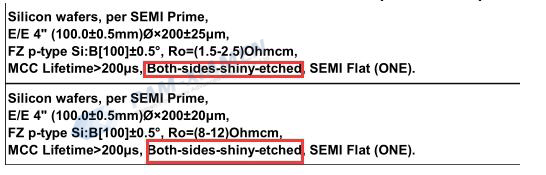
A: To get a shiny etched surface the silicon wafers shall be acid etched. The acid etching leads to the nice shiny surface (almost like the polished wafer surface), the alkaline etching leads to a matt surface.
For more information, please contact us email at victorchan@powerwaywafer.com and powerwaymaterial@gmail.com.
Found in 1990, Xiamen Powerway Advanced Material Co., Ltd (PAM-XIAMEN) is a leading manufacturer of semiconductor material in China.PAM-XIAMEN develops advanced crystal growth and epitaxy technologies, manufacturing processes, engineered substrates and semiconductor devices.PAM-XIAMEN’s technologies enable higher performance and lower cost manufacturing of semiconductor wafer.
Before 1990, we are stated owned condensed matter physics research center. In 1990, center launched Xiamen Powerway Advanced Material Co., Ltd (PAM-XIAMEN), now it is a leading manufacturer of compound semiconductor material in China.