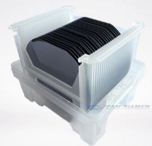
High quality GaAs based epistructures from PAM-XIAMEN – one of leading epitaxial wafer manufacturers are provided for the research, development and (potentially) later commercialization of very high efficiency light emitters for thermophotonic applications. In particular, commercially available GaAs based epi structure materials are offered long (up to micro second range in lattice matched InGaP/GaAs/InGaP structures) lifetimes and consistent quality. The material for a lock-in thermography can be characterized by electrical as well as optical and infrared thermometry based approaches. You can offer the structure of your GaAs epi-wafer to customize. More about our specifications please see as follows:

1. Structure of GaAs based Epitaxial Wafer for Light Emitters
PAMP16196-GAAS
| Layer | Material | Concentration | Thickness |
| 1 | Single polished n-type GaAs substrate / double polished p-type GaAs substrate | – | – |
| 2 | p-GaAs buffer | Not crucial | 100nm |
| 3 | p-GaAs contact layer | – | – |
| 4 | p-AlAs | – | – |
| 5 | p-GaAs | – | – |
| 6 | n-GaAs | – | – |
| 7 | n-GaAs | – | – |
| 8 | n-AlAs | – | – |
| 9 | n-AlxGa1-xAs | – | – |
| 10 | n-AlxGa1-xAs | – | – |
| 11 | i-GaAs | intrinsic | – |
| 12 | p-AlxGa1-xAs | – | – |
| 13 | p-AlxGa1-xAs | – | – |
| 14 | p-GaAs contact layer | – | 20nm |
2. About GaAs Diode Epitaxial Growth
For diode epi structure, the epi method adopted is MOCVD, not MBE. We aim for the materials with the highest possible quantum efficiency and smoothest layer interfaces possible, thus we may choose the growth method either MOCVD or MBE depending on abilities of our growth systems to provide the best quality material.
We will examine the crystal quality by HR-XRD, measure the sheet resistance uniformity and PL-mapping for GaAs epitaxial structures.
Here are PL-mappings of epitaxial wafers on n&p type GaAs substrate:

PL of N-type GaAs Epistructure

PL of P-type GaAs Epi structure
3. About P-type and N-type Substrate for above GaAs based Epi Structure
Regarding GaAs epilayers listed above, usually, the EPD of p-type substrate is more than that of n-type substrate. So for this epi-layer structure, the n type substrate also can be used for growing epilayers. If only described from the material structure, p-type substrate is the logical choice. Moreover, the GaAs-based epitaxy is intended to fabricate double diode structure and to evaluate the coupling quantum efficiency in the fabricated devices. Wet etching is used for the device fabrication with nearly all layers etched with customer’s selective solution. Therefore, from the material structure and device process, the 0 degree P-substrate with EPD lower than 900/cm2 is a good choice.
But some of the customers are interested in the quantum efficiency (QE) of the devices; they want to see the effect of the substrate EPD on the device performance, which can be achieved by growing the gallium arsenide epi structure on an N-type substrate with presumably lower EPD (less than 100/cm2). While the possibility is not ideal since the substrate no longer takes part in current spreading, and the resistive losses are somewhat increased, it should be ok for the purpose of double diode structure due to the thick p-type layer on top of the substrate. Thus, in this case, GaAs(100) off 15 degree substrate and 0-degree n-type substrate can be used. If the 0-degree n-substrate does not have a substantially larger EPD or if it simplifies the epitaxial growth process, the 0-degree n-substrate would be slightly preferred.
For more information, please contact us email at victorchan@powerwaywafer.com and powerwaymaterial@gmail.com.

