تقدم PAM-XIAMEN GaN على رقاقة HEMT السليكونية للطاقة ، الوضع E. نظرًا لأن خاصية التشغيل العادي ستزيد من تعقيد تصميم الدائرة واستهلاك الطاقة ، فإن تصميم HEMT المحسن (الوضع E) الذي يتم إيقاف تشغيله تحت انحياز الشبكة الصفري سيكون أمرًا حاسمًا لتطوير تطبيق GaN-on-Silicon HEMT في مجال الطاقة.
1. هياكل E-MODEالجاليوم HEMTعلى ركيزة السيليكون
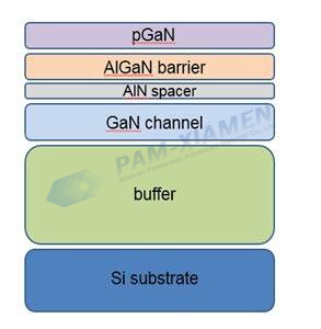
رقم 1 GaN على هيكل HEMT فوق المحور السليكوني
| GaN على حجم epitaxy HEMT السيليكون | 2 ، 4 ، 6 ، 8 |
| هيكل AlGaN / GaN HEMT | راجع 1.2 |
| كثافة 2DEG المتبقية (Vg = 0 V) | <1e18 / سم 3 |
| AFM RMS (نانومتر) من 5x5um2 | <0.25 نانومتر |
| القوس (أم) | <= 30 ميكرومتر |
| استبعاد الحافة | <5 مم |
| p-GaN | / |
| طبقة غطاء u-GaN | / |
| آل التكوين | 20-30٪ |
| طبقة الحاجز AlGaN | / |
| قناة GaN | / |
| المخزن المؤقت AlGaN | / |
| مادة الركيزة | ركيزة السيليكون |
| سمك رقاقة Si (ميكرومتر) | 675 ميكرومتر (2 ″) ، 1000 ميكرومتر (4 ″) ، 1300 ميكرومتر (6 ″) ، 1500 ميكرومتر (8 ″) |
رقم 2 4-inch GaN / Si Epi-Wafer PAM200211-HEMT
| هيكل GaN / Si HEMT Epi | ||
| طبقة | مادة | سماكة |
| 6 | p-GaN ، Mg-doped | – |
| 5 | AlN | – |
| 4 | AlGaN | – |
| 3 | AlN | – |
| 2 | GaN (طبقة القناة) | – |
| 1 | عازلة (آل ، جا) ن | > = 4 أم |
| المادة المتفاعلة | Si (111) ، سمك 1000 +/- 25 ميكرومتر ، انحراف أقل من 10 ميكرومتر | |
ملاحظة:
1 / في الوقت الحاضر ، هيكلنا القياسي AlGaN 12NM ، 25٪ Al لديه تركيز ناقل المعلمة المقابل> 6e12 ، التنقل> 2000 ، RS ~ 500 ، أفضل بكثير ؛
2 / تركيز المنشطات المغنيسيوم الحالي هو ~ 2e19 وتركيز التنشيط ~ 4e17.
Features of GaN on Si Epiwafers for power:
High uniformity and good repeatability;
Low leakage current with excellent;
2DEG transport properties;
Breakdown voltage ≥ 650 V;
RoHS compliant
Typical Applications of Si based GaN Epiwafers:
Suitable for power HEMTs and low cost CMOS process;
Suitable for power diodes
2. ما هو E Mode GaN على Silicon HEMT؟
يمكن أن يؤدي تغيير بنية عملية GaN على بوابة HEMT السليكونية لتبديل قطبية جهد العتبة إلى إنتاج جهاز GaN HEMT محسن (من النوع E). الغرض من تغيير هيكل العملية هو استنفاد 2DEG تحت البوابة بشرط عدم وجود جهد مطبق ، بحيث يمكن تعزيز جهد العتبة الأمامية بواسطة 2DEG لتشكيل قناة. بوابة GaN المشبعة على شكل P هي هيكل مشابه للديود في هيكل البوابة ، ويتم رفع جهد العتبة بواسطة انخفاض جهد الصمام الثنائي.
حاليًا ، هناك ثلاث طرق رئيسية لاستخدام بوابة من النوع p لتحقيق وضع HEMT المعتمد على GaN:
- تتمثل الطريقة الأولى للبوابة من النوع p بشكل أساسي في استخدام الطبقة الفوقية من النوع p بالكامل على طبقة الحاجز ، ثم حفر الطبقة من النوع p تحت البوابة والاحتفاظ بها لتحقيق التعزيز ؛
- والثاني هو تقليم الطبقة الفوقية من النوع p ، ثم الاحتفاظ بطبقة من النوع p تحت البوابة ، وحفر معظم الطبقة من النوع p في المنطقة غير ذات البوابة ، مع ترك 5-20 نانومترًا من الطبقة من النوع p . أثناء عملية التنميش ، تلحق البلازما الضرر بالواجهة وتؤثر على استقرار GaN على جهاز طاقة السيليكون ؛
- الطريقة الثالثة للبوابة من النوع p هي عمل epitaxy ثانوي في منطقة البوابة على طبقة الحاجز لتنمية البوابة من النوع p.
3. الأسئلة الشائعة حول GaN على Si Wafer للطاقة ، الوضع E
س 1:حول المعالجات السطحية لـ E-mode GaN على رقاقة Si HEMT: هل يمكنك أيضًا أن تعطينا بعض التلميحات للتغلب على هذه المشكلة الصعبة؟ خاصة عملية البوابة في أذهاننا. لسنا متأكدين تمامًا من المعالجات قبل تبخر البوابة المعدنية.
A: Concerning the surface of GaN on Si HEMT wafer, organic treatments are important after the pGaN etching, to repair the etched surface.
س 2:بالنسبة إلى GaN على هيكل Si epi لـ HEMT في الوضع E ، أجرينا أيضًا بعض عمليات المحاكاة وحققنا نتائج مماثلة في عمليات المحاكاة. أعني أن 13 نانومتر من حاجز AlGaN سيكون جيدًا للقيمة V المتوقعة. يمكنك الحصول على 180mA / مم ولكن في أي مسافة DS تلاحظ هذه الكثافة الحالية؟
وفقًا لعمليات المحاكاة التي أجريناها ، يعد تقليل سمك AlGaN إلى 13 نانومتر أمرًا جيدًا ولكن لكي نكون آمنين ، نحتاج أيضًا إلى الحفاظ على كسر Al mole عند 0.18. هل لديك أي توقعات إلى أي مدى سيغير هذا IDSS؟
A: Our source to drain distance is ~25 μm based on the HEMT epitaxial structure. Concerning the Idss of 13 nm Al(0.18) GaN barrier, it is difficult to say, as it is also influenced by the etching accuracy. For your reference, we have worked on a device with 12 nm Al(0.15)GaN barrier, the Idss is ~72 mA/ mm.
س 3:حول الأجهزة القائمة على GaN-on-Si مع جهد العتبة ، لقد جربنا معادن بوابة مختلفة (Pd ، tungsten ، Ni ، NiAu ، Ti ، إلخ) ولكنها دائمًا 0.7 فولت. نحتاج إلى زيادته حتى 1.2 فولت ، هل لديك أيضًا بعض التوصيات حول هذه المشكلة؟ سيساعدك توجيهك كثيرًا.
A: Concerning the breakdown voltage (BV): Wafers with the same/similar epi structure of GaN/Si HEMT is always processing in our own fab, and a stable BV output is obtained, with BV >650 V (Ieakage current Ids < 1 μA). A higher BV should be achieved by proper surface treatments and optimized passivation layer.
س 4:نحن نفكر في تعديل سمك AlGaN لبنية GaN HEMT لزيادة V. ما رأيك؟ أو ربما يمكنك اقتراح بعض الأشياء الأخرى لزيادة V.
A: Concerning the threshold voltage Vth of E-mode GaN/Si HEMT wafer: We believe the Vth can be enhanced by reducing the barrier thickness. We can obtain devices with Vth >1.5 V easily in our fab, with a ~13 nm Al0.2Ga0.8N barrier, while a relative high on state current can still be maintained (>180 mA/ mm). In your case, the AlGaN barrier is a bit thicker (18 nm), which may limit the Vth values to be < 1 V.
Q5: Do we need any kind of activation for Mg doping or did you already activated the doping in HEMT wafer of GaN on Si?
A: We already activated the doping in GaN-on-Si HEMT wafer.
Q6: We are still working on optimizing the process on your wafer. Till now we were able to achieve 420 V breakdown with the PGaN E mode wafer.
What is your estimation about breakdown voltage? How high we can go? I remember that you’ve told me that 650V may be abit difficult with E mode.
Do you have some progress on epi growth in the mean time? Is it possible to purchase a D mode wafer with 650V breakdown?
A: The breakdown voltage can reach to 1000V for both D mode and E mode HEMT wafer.
Q7: I remember that the vertical breakdown can go up to 1000V and we also measured about 900V with one of the samples. For the 600v operation you’ve suggested D mode. I understand that E mode will not be able to reach that value. Am I mistaken? Do you have any hints for us for achieving 600V by E mode wafers?
A: In 600v operation, we suggest use D mode HEMT wafer, which is more suitable in this voltage, but it doesn’t mean that breakdown voltage only reach to 600v, as mentioned, both can reach to 1000v.
Q8: Currently we are working on improving the breakdown voltage of the devices with your GaN on Si HEMT wafer. We obtained ~350V but we are searching the ways to reduce the leakages to improve the breakdown. But in the mean time we have problem with the threshold voltage. We need to have more positive voltages. I need your help and suggestions to improve the results.
What I have in mind is to decrease the AlGaN barrier thickness a bit but compensating the Ns loss with increasing the Al composition just a bit. In our opinion this should improve the threshold voltage of the devices. What do you think? We may order another wafer to improve these parameters.
Do you have any suggestions to improve the breakdown voltage of the device?
A: RE: the breakdown voltage of HEMT devices on GaN/Si wafer:
The wafer we have delivered to you is based on our HV buffer, which has a vertical breakdown voltage > 1000 V (@I < 1 uA/ mm2).
Actually, according to the devices fabricated on this epi structure, in our own fab, the off state leakage is Ids< 0.1 uA/ mm, while Vds = 650 V (Lds=15 um).
Both epi buffer and chip process contribute to the leakage, so we suggest you to check the chip process, especially the passivation layer, which is also critical for the leakage.
RE: the Vth of devices on GaN on Silicon HEMT wafer:
A thinner barrier layer will help increase the Vth for sure.
we can reduce the AlGaN (20% Al) thickness to 12.5 nm for you (the previous one was ~ 18 nm).
A Vth> 2 V (@Ids~10 uA/ mm) has been demonstrated in our fab, based on this structure.
Although it will sacrifice the Rs, a Rs value of ~550 ohm/sq is obtained.
By the way, the chip process, especially gate material, is also important for Vth.
Q9: I appriciate your reply. Thank you. We don’t face a problem with vertical breakdown we also measure about 1kV. But the DS leakage (we use LDS12um) is higher and we cannot achieve 650V.
To my observation our main problem comes from the gate leakage. And as you’ve stated gate material affects this leakage. We use Ni/Au as gate metal. But your little guidance will be much appriciated. What may be your suggestion to improve the gate leakage and the Vth as well? Do you use ALD or similar dielectric under the gate metal? Which metal structure do you use? What kind of things do you suggest to improve the gate contact?
A: RE: the gate metal for GaN HEMT device fabrication:
Our production line is “Au” free, so no Au is used, and also, Ni/Au contact usually gives high gate leakage.
Three types of gate contact may improve Vth: Ni, W (wolfram), or TiN (our option).
Concerning the leakage:
We measure the off state leakage at Vg = 0 V.
Actually, it depends on the Vth, if your Vth is close to 0 V, leakage at Vg=0V is high, as the device is not complete “turn off”; if the Vth > 1.5 V, our device gives low leakage (sub uA) @ Vg = 0 V.
Please be careful with the etching defects, which may also contribute to the off state leakage.
We hope the above information can help.
Q10: I would like to insert an 1 nm AlN layer between p-GaN and AlGaN. Is it possible?
A: No problem to inser an 1nm AlN layer between p-GaN and AlGaN, but which can not help to stop etch.

لمزيد من المعلومات ، يرجى الاتصال بنا على البريد الإلكتروني على victorchan@powerwaywafer.com و powerwaymaterial@gmail.com.