GaN HEMT رقاقة الفوقي
Gallium Nitride (GaN) HEMTs (High Electron Mobility Transistors) are the next generation of RF power transistor technology. Thanks to GaN technology, PAM-XIAMEN now offer AlGaN/GaN HEMT Epi Wafer on sapphire or Silicon, and AlGaN/GaN on sapphire template.
- وصف
وصف المنتج
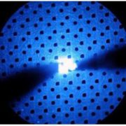
GaN HEMT epitaxial wafer is a multilayer film grown epitaxially on a substrate, which usually includes a nucleation layer, a transition layer, a buffer layer, a channel layer, a barrier layer, a cap layer, and a passivation layer from bottom to top. The nucleation layer, like AlGaN or AlN, is used to prevent the substrate material from diffusing into the GaN epitaxial layer. The transition layer may contain hierarchical AlGaN, AlN/GaN superlattice or multilayer AlN to balance the stress between the GaN and the substrate. The higher the Al content in the barrier layer of AlGaN, the higher the 2DEG concentration at the heterojunction. Meanwhile, the lower the threshold voltage of the device, and the higher the current capacity. As the Al ratio increasing, the degree of heterogeneous crystal lattice mismatch will be higher, resulting in a decrease in gallium nitride HEMT electron mobility and a decrease in current capacity.
The High Electron Mobility Transistor (HEMT) is developed based on GaN with unique heterostructure and two-dimensional electron gas. The GaN HEMT advantages include high breakdown strength, low on-resistance and faster The switching speed, which is very suitable for medium and low voltage and medium and small power systems, such as travel adapters, wireless chargers, AC-DC converters, smart home appliances, etc. The epitaxial wafer with HEMT structure is more attractive currently for high-frequency converters, in which GaN HEMT breakdown voltage is 600~650 V. With the rapid development of gallium nitride HEMT epi technology, the price of GaN HEMT devices will be competitive, which can gain large GaN HEMT market for GaN HEMT manufacturers. Moreover, due to the gallium nitride HEMT reliability, it can be widely used in industrial fields, such as photovoltaic inverters, energy storage systems, and electric vehicles.
1. GaN HEMT Material: Available size:2”,4”,6”,8”:
More specific parameters of gallium nitride HEMT wafer for D-mode GaN HEMTs, E-mode GaN HEMTs, GaN HEMT power amplifier and RF, please refer to:
الجاليوم على Si للسلطة ، وضع D
الجاليوم على Si للسلطة ، الوضع E
We are expert in HEMT structure, we also offer GaN HEMT epi wafer for many years.
For silicon substrate, we need to know if you grow GaN HEMT on silicon for POWER or RF, it is different. If needed, please contact victorchan@powerwaywafer.com for details.
For SiC, you should use semi-insulating.
Or you can buy AlGaN/GaN HEMT structure on these three structure from us.
2. Now we show you an example as follows:
2.1 2 ″ (50.8 مم) GaN HEMT Epitaxial Wafers
We offer 2″(50.8mm) gallium nitride HEMT Wafers, the GaN HEMT structure is as follows:
الهيكل (من الأعلى إلى الأسفل):
* غطاء الجاليوم غير المغطى (2 ~ 3nm)
AlxGa1-xN (18 ~ 40 نانومتر)
AlN (طبقة عازلة)
GaN غير مخدر (2 ~ 3um)
الركيزة الياقوت
* يمكننا استخدام Si3N لاستبدال GaN في الأعلى ، التصاق قوي ، مغلف بالخرخ أو PECVD.
2.2 AlGaN/GaN HEMT Epi Wafer on sapphire/GaN
| الطبقة رقم | تركيب | سماكة | X | المقوي | تركيز الناقل |
| 5 | الجاليوم | 2 نانومتر | – | – | – |
| 4 | AlxGa1 – xN | 8 نانومتر | 0.26 | – | – |
| 3 | AlN | 1 نانومتر | غير مخدر | ||
| 2 | الجاليوم | n1000 نانومتر | غير مخدر | ||
| 1 | طبقة عازلة / انتقال | – | – | ||
| المادة المتفاعلة | السيليكون | 350µm / 625µm | – | ||
2.3 2″(50.8mm),4″ (100mm)AlGaN/GaN HEMT Epi Wafer on Si
2.3.1 Specifications for Aluminium Gallium Nitride (AlGaN) / Gallium Nitride (الجاليوم) ترانزستور التنقل الإلكتروني العالي (HEMT) على الركيزة السليكونية.
| المتطلبات | مواصفات |
| AlGaN / GaN HEMT Epi Wafer على Si | |
| هيكل AlGaN / GaN HEMT | راجع 1.2 |
| الركيزة المواد | السيليكون |
| اتجاه | <111> |
| طريقة النمو | منطقة عائمة |
| نوع التوصيل | ص أو ن |
| الحجم (بوصة) | 2 "، 4" |
| سمك (ميكرون) | 625 |
| المؤخر | الخام |
| المقاومة (Ω-cm) | >6000 |
| القوس (ميكرون) | ≤ ± 35 |
2.3.2 Epi structure: Crack-free Epilayers
| الطبقة رقم | تركيب | سماكة | X | المقوي | تركيز الناقل |
| 5 | الجاليوم | 2 نانومتر | – | – | – |
| 4 | AlxGa1 – xN | 8 نانومتر | 0.26 | – | – |
| 3 | AlN | 1 نانومتر | غير مخدر | ||
| 2 | الجاليوم | n1000 نانومتر | غير مخدر | ||
| 1 | طبقة عازلة / انتقال | – | – | ||
| المادة المتفاعلة | السيليكون | 350µm / 625µm | – | ||
2.3.3 Electrical Properties of the AlGaN/GaN HEMT structure
2DEG Mobility (at 300 K): 8001،800 cm2 / Vs
2DEG كثافة حامل صفائح (عند 300 كلفن): .90.9 × 1013 سم -2
خشونة RMS (AFM): ≤ 0.5 نانومتر (5.0 µm × 5.0 Aream منطقة المسح)
2.4 2″(50.8mm)AlGaN/GaN on sapphire
لمواصفات AlGaN / GaN على قالب الياقوت ، يرجى الاتصال بقسم المبيعات لدينا: sales@powerwaywafer.com.
GaN HEMT Applications: Used in blue laser diodes, ultraviolet LEDs (down to 250 nm), and AlGaN/GaN HEMTs device.
3. Explanation of AlGaN/Al/GaN HEMTs:
يتم تطوير Nitride HEMTs بشكل مكثف للإلكترونيات عالية الطاقة في تطبيقات التضخيم عالي التردد وتبديل الطاقة. غالبًا ما يتم فقد الأداء العالي في تشغيل التيار المستمر عند تبديل HEMT - على سبيل المثال ، ينهار التيار عند نبض إشارة البوابة. يُعتقد أن هذه التأثيرات مرتبطة بحبس الشحن الذي يخفي تأثير البوابة على التدفق الحالي. تم استخدام لوحات المجال على أقطاب المصدر والبوابة لمعالجة المجال الكهربائي في الجهاز ، مما يخفف من مثل هذه الظواهر الانهيار الحالي.
4. GaN EpitaxialTechnology — Customized GaN epitaxy on SiC,Si and Sapphire substrate for HEMTs, LEDs:
GAN HEMT الفوقي رقائق (GAN EPI-رقائق)
PAM XIAMEN Offers Epitaxial growth of AlGaN/GaN based HEMT on Si wafers
5. GaN Device:
الجاليوم HEMT
6. Test Characterization Equipment:
مقاومة ورقة تماس
رسم خرائط سمك طبقة رقيقة ليزر
درجة حرارة عالية / رطوبة عالية عكس الانحياز
صدمة حرارية
DIC Nomarski مجهر
مجهر القوة الذرية (AFM)
مسح عيب السطح
ارتفاع درجة الحرارة عكس التحيز
4PP مقاومة الورقة
التنقل قاعة تلامس
دورة درجة الحرارة
حيود الأشعة السينية (XRD) / الانعكاس (XRR)
سمك جهاز القطع
مقياس البروفيل
اختبار السيرة الذاتية
7. Foundry Fabrication:
we also offer foundry GaN HEMT fabrication in the following process as follows:
MOCVD Epitaxy
الاخرق المعدني / الشعاع الإلكتروني
حفر جاف / رطب / عازل كهربائي
الأغشية الرقيقة PECVD / LPCVD / الاخرق
هيئة الطرق والمواصلات / فرن الصلب
الليثوغرافيا الضوئية (0.35um min. CD)
زرع الأيونات
Remark:
The Chinese government has announced new limits on the exportation of Gallium materials (such as GaAs, GaN, Ga2O3, GaP, InGaAs, and GaSb) and Germanium materials used to make semiconductor chips. Starting from August 1, 2023, exporting these materials is only allowed if we obtains a license from the Chinese Ministry of Commerce. Hope for your understanding and cooperation!
More fabrication services, please visit: GaN Fabrication Services for HEMT Devices
الجاليوم / كربيد HEMT برنامج التحصين الموسع-رقائق
Aluminium gallium arsenide epi wafer
650V GaN FETs Chip for Fast Charge
GaN MOSFET Structure:
GaN MOSFET Structure on SiC Substrate
More about GaN HEMT structures, please read:
ربما يعجبك أيضا…
-
طليق الركيزة الجاليوم
أنشأت PAM-شيامن التكنولوجيا لتصنيع قائما بذاته (نيتريد الغاليوم) الجاليوم الركيزة ويفر، التي هي لUHB-LED وLD. نما بنسبة تكنولوجيا هيدريد مرحلة البخار تنضيد (HVPE)، لدينا الركيزة الجاليوم ديها منخفض الكثافة عيب.
-
GaSb يفر
PAM-XIAMEN offers Compound Semiconductor GaSb wafer – gallium antimonide which are grown by LEC(Liquid Encapsulated Czochralski) as epi-ready or mechanical grade with n type, p type or semi-insulating in different orientation(111) or (100).
-
شركة جنرال الكتريك (الجرمانيوم) بلورات واحدة ويفر
تقدم شركة PAM-XIAMEN رقائق الجرمانيوم مقاس 2 و3 و4 بوصات و6 بوصات، وهي اختصار لرقائق Ge التي تنمو بواسطة VGF / LEC. يمكن أيضًا استخدام رقاقة الجرمانيوم من النوع P وN المخدرة بشكل خفيف في تجربة تأثير هول. في درجة حرارة الغرفة، يكون الجرمانيوم البلوري هشًا وله القليل من اللدونة. الجرمانيوم له خصائص أشباه الموصلات. يتم تطعيم الجرمانيوم عالي النقاء بعناصر ثلاثية التكافؤ (مثل الإنديوم والجاليوم والبورون) للحصول على أشباه موصلات الجرمانيوم من النوع P؛ ويتم تخدير العناصر الخماسية التكافؤ (مثل الأنتيمون والزرنيخ والفوسفور) للحصول على أشباه موصلات الجرمانيوم من النوع N. يتمتع الجرمانيوم بخصائص جيدة لأشباه الموصلات، مثل حركة الإلكترون العالية وحركة الفتحات العالية. -
تطفو منطقة أحادي البلورية السيليكون
يمكن لشركة PAM-XIAMEN أن تقدم رقاقة السيليكون ذات المنطقة العائمة، والتي يتم الحصول عليها بطريقة المنطقة العائمة. يتم الحصول على قضبان السيليكون أحادية البلورية من خلال نمو المنطقة العائمة، ومن ثم معالجة قضبان السيليكون أحادية البلورية إلى رقائق السيليكون، والتي تسمى رقائق السيليكون ذات المنطقة العائمة. نظرًا لأن رقاقة السيليكون المنصهرة في المنطقة ليست على اتصال مع بوتقة الكوارتز أثناء عملية السيليكون في المنطقة العائمة، فإن مادة السيليكون تكون في حالة معلقة. وبالتالي، فهو أقل تلوثًا أثناء عملية ذوبان السيليكون في المنطقة العائمة. محتوى الكربون ومحتوى الأكسجين أقل، والشوائب أقل، والمقاومة أعلى. إنها مناسبة لتصنيع أجهزة الطاقة وبعض الأجهزة الإلكترونية ذات الجهد العالي.
-
كربيد يفر الركيزة
The company has a complete SiC(silicon carbide) wafer substrate production line integrating crystal growth, crystal processing, wafer processing, polishing, cleaning and testing. Nowadays we supply commercial 4H and 6H SiC wafers with semi insulation and conductivity in on-axis or off-axis, available size:5x5mm2,10x10mm2, 2”,3”,4”, 6” and 8″, breaking through key technologies such as defect suppression, seed crystal processing and rapid growth, promoting basic research and development related to silicon carbide epitaxy, devices, etc.
-
LED الفوقي رقاقة الجاليوم مقرها
الجاليوم PAM-شيامن (نيتريد الغاليوم) ومقرها الصمام رقاقة الفوقي هو لارتفاع سطوع الثنائيات جدا الزرقاء والخضراء التي ينبعث منها ضوء (LED) والثنائيات الليزر (LD) التطبيق.
-
الغاليوم Epiwafer
PAM-XIAMEN is manufacturing various types of epi wafer III-V silicon doped n-type semiconductor materials based on Ga, Al, In, As and P grown by MBE or MOCVD. We supply custom GaAs epiwafer structures to meet customer specifications, please contact us for more information.
-
قوالب الجاليوم
تتكون المنتجات قالب PAM-شيامن للطبقات البلورية (نيتريد الغاليوم) قوالب الجاليوم، (الألومنيوم نيتريد) قالب ن.، (الألومنيوم نيتريد الغاليوم) قوالب ألجان و(الإنديوم نيتريد الغاليوم) قوالب InGaN، التي تترسب على الياقوت


