Silicon carbide has a variety of crystal types, but the silicon crystal structure the market needed is mainly 4H-SiC. So the silicon carbide crystal growth in crystal types is a defect. To a certain extent, it can be distinguished by the naked eye. A more accurate measurement method for testing the silicon carbide crystal distribution is Raman spectroscopy: Raman spectroscopy has characteristics for crystals, and the peak positions of the light emitted by different crystals are different.
1. What is Raman Spectroscopy?
في عام 1928 ، اكتشف العالم الهندي رامان تشتت رامان في تجربة دراسة طيف تشتت البنزين السائل. مطيافية تشتت رامان ، بعبارات بسيطة ، هي استخدام شعاع من الضوء الساقط على مادة ما ، وتردد الضوء الساقط هو v ، وتكرار الضوء المنتشر الناتج سيكون v ، v + Δv1 ، v-Δv1 ، v + Δv2 و v-Δv2 وما إلى ذلك. هذه Δv1 ، Δv2 ، إلخ. v لها خصائص. بمعنى آخر ، كل مادة لها اختلاف معين (موضع الذروة ، شدة الذروة) ، والذي يسمى تحول رامان (الضوء المنبعث مطروحًا منه الضوء الساقط).
على سبيل المثال ، طيف رامان لـ 4H-SiC هو:
| تحول رامان (سم-1) | الموجة الصوتية المستعرضة E2 | الموجة الصوتية المستعرضة E2 | الموجة الصوتية المستعرضة A1 | الموجة الصوتية المستعرضة E2 | الموجة الصوتية المستعرضة A1 | A1 موجة صوتية طولية | LOPC | LOPC |
| 4H- كربون | 194.958 | 204.034 | 610.031 | 776.489 | 796.861 | 963.106 | 964.769 | 994.643 |
The table above shown here is the Raman shift. During the silicon carbide crystal distribution measurement, the computer will help to calculate it and process it as a Raman shift spectrum.
2. How to Test the Silicon Carbide Crystal Distrubution?
شروط الاختبار النموذجية هي: استخدام الليزر 532 نانومتر لليزر Ar + لمطياف LabRAM HR Raman ، يتم عرضه عموديًا ، وقوة الإثارة 200mW ، ووضع تجميع الضوء المتناثر هو وضع التشتت الخلفي. الضوء الساقط بأطوال موجية مختلفة له أعماق اختراق مختلفة. بشكل عام ، يبلغ حجم الليزر 266 نانومتر 0.2 ميكرون ، والليزر 325 نانومتر هو 2 ميكرومتر ، والليزر 514 نانومتر هو 30 ميكرومتر ، مما يعني أنه لا يمكن استخدام الضوء فوق البنفسجي إلا لقياس العينات الرقيقة.
Because the silicon carbide wafer has different positions, multiple measurements will be taken to obtain the silicon carbide crystal distribution:
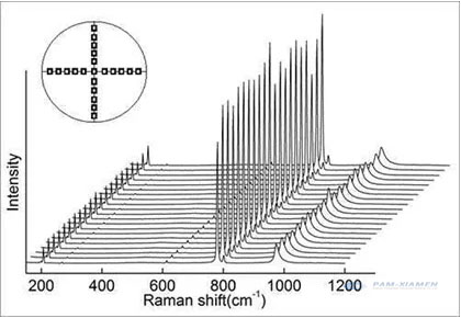
The data has three indicators: the position of the peak, the height of the peak (light intensity), and the width of the peak. Only when the peak position is completely matched, can it be 4H-SiC المؤهل. كما هو الحال مع XRD ، كلما كانت هناك قمم أخرى ، فهي مواد من مراحل أخرى ، وهذا عيب.
The difference in the position of the peak is due to the difference in the energy of the phonons brought about by the different silicon carbide crystal lattices, that is, the different frequencies. Each phonon has its corresponding energy level. The virtual energy level theory can be used to explain Raman (non-linear process):
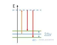
يمتص الجسيم الضوء الساقط إلى مستوى الطاقة الافتراضي (البرتقالي) ، ثم ينتقل مرة أخرى إلى مستوى طاقة اهتزازي (أحمر) يختلف عن مستوى الطاقة الأصلي. نظرًا لأن مستوى الطاقة العلوي هو مستوى طاقة افتراضي ، يمكن تغيير تواتر الضوء الساقط ، طالما أنه لا يتعارض مع مستوى الطاقة الحقيقي الأصلي.
تجدر الإشارة إلى أنه يمكن استخدام وضع LOPC (964.769 سم -1) لتحليل تركيز المادة الحاملة:
n = 1.25 * 1017cm-2 *(964.769cm-1-VLOPC measurement)
As the carrier concentration increases, the interaction between atoms and the lattice increases, which makes the Raman peak blue shift (smaller), the intensity decreases, and the width increases. This method is not as accurate as other methods and can only be used as an aid to analyze the silicon carbide crystal distribution.
3. Why not Use XRD to Measure Silicon Carbide Crystal Distribution?
X-rays are optical radiation generated by the transition of electrons in the inner layer of atoms under the bombardment of high-speed moving electrons, including continuous X-rays and characteristic X-rays. Silicon carbide single crystal can be used as X-ray gratings, and the coherent scattering produced by these large numbers of particles (atoms, ions, or molecules) will cause light interference, increasing or decreasing the intensity of scattered X-rays. Due to the superposition of scattered waves from a large number of particles, the beams that interfere with each other to produce the highest intensity are called X-ray diffraction lines.
للوفاء بشروط الحيود ، يمكن تطبيق صيغة Bragg: 2dsinλ = nλ.
تتسبب الحزمة الساقطة في إعادة إشعاع كل مبعثر لجزء صغير من شدته كموجة كروية. إذا تم ترتيب المشتتات بشكل متماثل مع الفاصل الزمني d ، فستتم مزامنة هذه الموجات الكروية فقط في الاتجاه الذي يكون فيه اختلاف طول المسار 2dsinθ مساويًا لعدد صحيح مضاعف لطول الموجة λ. في هذه الحالة ، ينحرف جزء من الحزمة الساقطة بزاوية 2θ ، مما ينتج عنه نقاط انعكاس في نمط الانعراج.
Use X-rays of known wavelengths to measure the θ angle to calculate the interplanar spacing d, which is used for X-ray structure analysis; the other is to use a silicon carbide seed crystal with a known d to measure the θ angle to calculate the characteristic X-ray wavelength, and then the elements contained in the sample can be found in the existing data.
The measurement formula is 2dSinθ=λ. While the d value among the cubic silicon carbide crystal is close, and the characteristic is not obvious enough, the accurate silicon carbide crystal distribution cannot be precisely determined. For these reasons, it is not suitable to use the XRD to measure the distribution of silicon carbide crystals.

لمزيد من المعلومات ، يرجى الاتصال بنا على البريد الإلكتروني على victorchan@powerwaywafer.com و powerwaymaterial@gmail.com.