Atomic Layer Deposition (ALD), also known as atomic layer epitaxy (ALE), is an atomic-scale thin film preparation technology. It can deposit ultra-thin films with uniform thickness, controllable thickness and adjustable composition. With the development of nanotechnology and semiconductor microelectronics, the size requirements of devices and materials are continuously reduced, and the aspect ratio in the device structure is continuously increased, requiring the thickness of the materials used to be reduced to the order of ten nanometers to several nanometers. Atomic layer deposition technology has gradually become an irreplaceable technology in related manufacturing fields. Its advantages determine that it has huge development potential and broader application space. Metallic silicon wafers by ALD can be provided by PAM-XIAMEN.
1. Working Principle of Atomic Layer Deposition Technology
The atomic layer deposition technology refers to a method of forming thin films by alternating pulses of gas-phase precursors into the reaction chamber and gas-solid phase chemical adsorption reaction on the surface of the deposition substrate. As shown in Figure 1, the atomic layer deposition process consists of two half-reactions A and B in four elementary steps:
1) Precursor A pulse adsorption reaction;
2) Purging excess reactants and by-products with inert gas;
3) Precursor B pulse adsorption reaction;
4) The excess reactants and by-products are purged by the inert gas, and then circulated in sequence to realize the layer-by-layer growth of the thin film on the surface of the substrate.
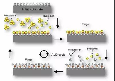
Figure 1. Working Principle of ALD
A wide variety of materials can be deposited by atomic layer deposition, such as:
Oxides: including HfO2, HfSiO, Al2O3, Ta2O5, TiO2, La2O3, SiO2, ZnO
Nitride, including TiN, TaN, AlN, SiNx, HfN
Metals, including Ru, Cu, W, Mo
2. Comparison of ALD, PVD and CVD
Compared with traditional thin film preparation technology, atomic layer deposition technology has obvious advantages. Traditional solution chemical methods and physical methods such as sputtering or evaporation (PVD) are not suitable for deposition and film formation on the surface of three-dimensional complex substrates due to lack of surface control or the existence of sputtered shadow areas. The chemical vapor deposition (CVD) method requires strict control of the precursor diffusion and the temperature uniformity of the reaction chamber, and it is difficult to meet the requirements of thin film uniformity and precise control of thickness. In contrast, ALD technology is based on surface self-limiting and self-saturating adsorption reactions, and has surface control. The bottom surface is deposited to form films, while still ensuring precise sub-monolayer film thickness control. Therefore, ALD technology is widely used in microelectronics, energy, information and other fields.
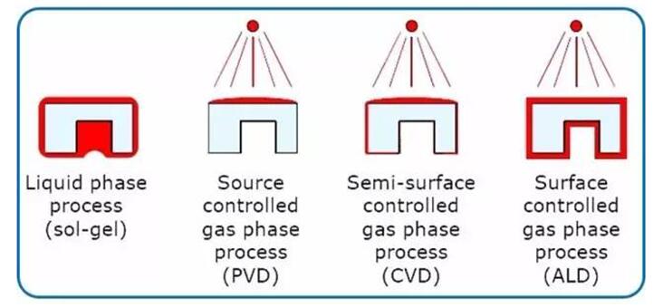
Figure 2. Comparison of ALD, PVD, CVD and so on
3. Basic Applications of Atomic Layer Deposition Technology
The development of atomic layer deposition technology is inseparable from the rise of the semiconductor industry. With the continuous improvement of chip integration, the size of various components continues to shrink, and the technology node of the semiconductor industry has entered the nano era. People also put forward higher and higher requirements for nano-scale thin film preparation technology compatible with semiconductor technology. The main applications of ALD technology include:
1) Transistor gate dielectric (high-k) and metalgate electrode;
2) Micro-electromechanical systems (MEMS);
3) Optoelectronic materials and devices;
4) Integrated circuit interconnect diffusion barrier;
5) Flat panel display (e.g. Organic light emitting diode material, OLED);
6) Interconnect barrier layer;
7) Interconnect copper electroplating deposition seed layer;
8) DRAM, MRAM dielectric layer;
9) Embedded capacitor;
10) Electromagnetic recording head;
11) Various types of thin films (<100nm).

For more information, please contact us email at victorchan@powerwaywafer.com and powerwaymaterial@gmail.com.