PAM-XIAMEN offers C-Plane Sapphire Substrate, single side polished or double side polished, please see below spec:
1. Specifications of C-Plane Sapphire Substrate
2” C-plane SSP Sapphire Substrate:
| No | Item | Specification |
| 1 | Material | High PurityAl2O3 |
| 2 | Diameter | 50.8+0.1mm |
| 3 | Thickness | 430土15um |
| 4 | TTV | ≤10μm |
| 5 | LTV | ≤1.5μm |
| 6 | Bow | -10~0μm |
| 7 | Warp | ≤10μm |
| 8 | Primary Flat Length | 16.0土1.0mm |
| 9 | Front Surface Roughness(Ra)| | Ra≤0.2nm |
| Back Surface Roughness(Ra) | 0.7~1.2μm | |
| 11 | Primary Flat Orientation | A-plane土0.2° |
| 12 | Surface Orientation | C-Plane(0001) off Angle 0.2o+0.1″(M-axis);0°+0.1″(A-axis) |
| 13 | Laser Mark | back side or frontside |
| 14 | Package | 25pcs/Cassette, Vacuum-sealed, Nitrogen- filled, Class-100 Cleanroom |
Remark: C-plane 0/ 0.1/0.3/ 0.5 deg. to the M plane, +/-0.1 deg. to the A-plane are all available.
3” C-plane SSP Sapphire Substrate: PAM200221-SAPPHIRE
| No | Item | specification |
| 1 | Material | High Purity Al2O3 |
| 2 | Diameter | 76.2土0.4mm |
| 3 | Surface Orientation | C-Plane(0001) off Angle0.2°+0.1*(M-axis);0*+0.1*(A-axis) |
| 4 | Primany Flat Orientation | A-plane土0.5° |
| 5 | Primary Flat Length | 220土1.0mm |
| 6 | Thickness | 500土25μm |
| 7 | TTV | ≤10μm |
| 8 | Bow | -10~0um |
| 9 | warp | ≤15μm |
| 10 | Front Surface Roughness(Ra) | Ra≤0.3nm |
| 11 | Back Surface Roughness(Ra) | 0.7~1.2um |
| 12 | Laser Mark | Back or Front Side (BacksidePreferred) |
| 13 | Package | 25pcs/Cassette, Vacuum-sealed, Nitrogen- filled, Class100 Cleanroom |
4” C-plane DSP Sapphire Substrate:PAM20-02-SAPPHIRE
| No | Item | Specification |
| 1 | Material | High Purity Al2O3 |
| 2 | Diameter | 100.0土0.2mm |
| 3 | Thickness | 650土20μm |
| 4 | Surface Onientation | C-Plane(0001) off Angle0.2*+0.1*(M-axis);O*tO.1″(A-axis) |
| 5 | Primary Flat Orientation | A-plane士0.2° |
| 6 | Primary Flat Length | 30.0土1.0mm |
| 7 | TTV | ≤10um |
| 8 | LTV | ≤1.5μm(5mm*5mm) |
| 9 | Bow | -15~0μm |
| 10 | Warp | ≤30μm |
| 11 | Front Surface Roughness(Ra) | Ra≤0.3nm |
| 12 | Back Surface Roughness(Ra) | Ra≤0.3nm |
| 14 | LaserMark | Back or Front Side(Backside Preferred) |
| 15 | Package | 25pcs/Cassette,Vacuum-sealed,Nitrogen- |illed,Class-100 Cleanroom |
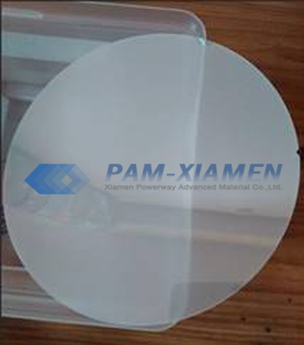
C-Plane Sapphire Substrate
2. Sapphire Wafer Applications
Because of its unique characteristics of high sound speed, high temperature resistance, high transparency and etc., sapphire wafers can be widely used. The customers bought them for some applications:
1) LED Fabrication: Sapphire substrate is widely used in growing GaN thin films to fabricate the LEDs since it can withstand the high temperature during epitaxial growth.
2) RF and Microwave Integrated Circuits: Low dielectric loss of sapphire makes it ideal for RF and microwave ICs, and high frequency devices, such as resonator and filter.
3) Optoelectronics: The properties of optical transparency and hardness make sapphire wafer is able to produce lenses, windows, and other optical components.
4) High Temperature Electronics: Sapphire wafers of high melting point and ability to withstand harsh environments can be used for fabricating electronics, which operate under harsh conditions.
5) Biomedical Usage: Due to its chemical inertness, bio-compatibility and radio-resistance, sapphire is ideal for biomedical usages, like surgical tools, medical implants.
6) R&D: Researchers and companies also buy sapphire substrates for research and development to developing new materials and technologies.
7) Silicon-On-Sapphire Circuits: The sapphire substrates can be used to grow silicon thin film, that is silicon-on-sapphire technology. In this technology, sapphire substrate plays as an insulator, reducing parasitic capacitance, and is widely used in producing faster and more efficient integrated circuits.
For more information, please contact us email at victorchan@powerwaywafer.com and powerwaymaterial@gmail.com.