The objective of this work is to analyze the effects of argon ion irradiation process on the structure and distribution of Te inclusions in Cd1-xZnxTe crystals. The samples were treated with different ion fluences ranging from 2 to 8 × 1017 cm−2. The state of the samples before and after irradiation were studied by Scanning Electron Microscopy (SEM), Atomic Force Microscopy (AFM), Cathodoluminescence, Photoluminescence, and micro-Raman spectroscopy. The effect of the irradiation on the surface of the samples was clearly observed by SEM or AFM. Even for small fluences a removal of polishing scratches on the sample surfaces was observed. Likely correlated to this effect, an important enhancement in the luminescence intensity of the irradiated samples was observed. An aggregation effect of the Te inclusions seems to occur due to the Ar bombardment, which are also eliminated from the surfaces for the highest ion fluences used.
Highlights
► After argon irradiation using low fluence, the defects on surface were removed.
► The PL intensity increases after irradiation. This increase should be related to the improved quality of the CdZnTe surfaces.
► Irradiation process lead to an elimination of Te precipitates from the surfaces of the CdZnTe samples.
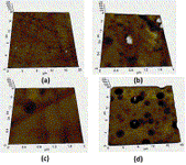
Fig. 1. AFM images of CZT samples: no irradiated (a) and irradiated with fluences of 2 × 1017 cm−2 (b), 4 × 1017 cm−2 (c) and 8 × 1017 cm−2 (d).
Source: Journal of Alloys and Compounds
If you need more information about Characterization of CdZnTe after argon ion beam bombardment, please visit our website:https://www.powerwaywafer.com/, send us email at sales@powerwaywafer.com or powerwaymaterial@gmail.com.