
Characterization of A Novel Indium Phosphide (InP) Charged Particle Detector Using a 120 GeV Proton Beam *
1. Abstract
Thin-film detectors incorporating semiconductor materials beyond silicon hold the potential to leverage their unique material properties and offer advantages such as faster response times, operation at room temperature, and radiation hardness. To explore this potential, promising candidate materials were selected and particle tracking detectors were fabricated. This study produced an indium phosphide (InP) detector with a metal-insulator-metal (MIM) structure for particle tracking. The detector was tested at Fermi National Accelerator Laboratory using radioactive sources and high-energy proton beams. In addition to its simple design and fabrication process, the InP particle detector exhibits a very fast response time to 120 GeV protons, reaching hundreds of picoseconds, comparable to ultra-fast silicon detectors. This rapid timing response is attributed to InP’s high electron mobility. This material characteristic can be utilized to construct novel detectors with ultra-high performance.
2. InP Detector Preparation
A 2-inch, 350um thick, single-crystal, single-sided polished InP:Fe wafer from PAM-XIAMEN was cut into 1 x 1 cm wafers, then cleaned for 2 minutes in a 120°C piranha liquid. The front side of the chip was spin-coated with Microposit S1818 photoresist and patterned using a Heidelberg MLA150. A 4 x 4 array of 200 x 200um pads was patterned on the front side of the chip. Electrodes were evaporated onto the InP chip using electron-beam evaporation (Temescal FC2000). A 10nm thick chromium adhesion layer was deposited, followed by an additional 100nm of gold to allow wire bonding. The backside electrode was deposited using sputtering coating (AJA metal sputtering system). A single backside electrode covered the entire chip, with chromium and gold thicknesses of 20nm and 100nm, respectively. Finally, laboratory electrical and radiation source measurements, as well as test beam measurements, were conducted.

Fig. 1 I-V temperature study of the InP:Fe detector

Fig. 2 Test beam data of the InP detector
3. Conclusion
A charged particle detector was fabricated on a semi-insulating InP wafer. The InP detector was compared with detectors using CdZnTe and single-crystal diamond, as shown in Fig. 3:
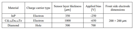
Fig. 3 Device performance of charged particle detectors on InP, CdZnTe and diamond
The detector was tested at Fermi National Accelerator Laboratory using an in-house radiation source and a 120GeV proton test beam. The InP-based detector shows great promise as a charged particle detector, exhibiting a very fast timing response in the picosecond region. The spectrum shows linear energy calibration using four different energy sources, with an energy resolution of approximately 28%. The detector provides good performance with a nominal optimized design and architecture as the first iteration. The measured rise time is comparable to fast silicon detectors such as low-gain avalanche diodes (LGAD). The simple device design can convert to lower manufacturing costs compared to some silicon detectors. Further improvements can be made by integrating InP with existing CMOS technologies, such as faster response times and cleaner signals. The sensing layer does not need to be thinned to very low thicknesses that could lead to durability issues, which is necessary for fast response in some silicon detectors.

For more information, please contact us email at [email protected] and [email protected].