After the growth, the silicon carbide single crystal is crystal ingot with surface defects, which cannot be directly used for epitaxy. Therefore, it requires chemical mechanical polishing on silicon carbide. Among the processing skills, spheronization makes the crystal ingot into a standard cylinder; wire cutting will cut the ingot into wafers; various characterizations ensure the direction of processing, and polishing is to improve the quality of the wafer.
The surface of the wafer will be damaged. The damage is caused by the defects of the original crystal growth and the damage in the previous processing steps. For partial damage, there are four methods to solve: ignoring, replacing, repairing and removing. Regardless of the damage layer on the silicon carbide surface, it will affect the yield of the device; replacing the chip is not a wise choice, because it will impact on your reputation among the industry; Repairing is actually growing again, and there is no low-cost solution now; and removal is a feasible option. Use a certain material to improve the overall quality of the material.
There are four methods to remove the damage layer on the SiC surface:
- Mechanical polishing, simple but will leave scratches, suitable for initial polishing;
- Chemical Mechanical Polishing on silicon carbide, which introduces chemical corrosion to remove scratches, suitable for fine polishing;
- Hydrogen etching, complicated equipment, often used in HTCVD process;
- Plasma-assisted polishing, complicated equipment, not commonly used.
Why Choose Chemical Mechanical Polishing for SiC Wafer?
Pure mechanical polishing will produce the wafer with scratches, pure chemical polishing will produce the crystal with non-uniform corrosion, and chemical mechanical polishing on silicon carbide will produce the wafer with a high quality and a competitive price. The working principle of CMP: The rotating wafer/silicon wafer does relative motion on the rotating polishing pad with a certain pressure, and the planarization requirements are achieved by the combination of the mechanical grinding effects of the nano-abrasive in the polishing liquid and the chemical effects of various chemical reagents.
The materials used in this process mainly include polishing fluids and polishing pads. After using the polishing pad, the wafer will deform. The surface becomes smooth, the pores are reduced and blocked, which make the polishing rate reduced. The wafer must be trimmed to restore its roughness and improve the ability to transfer the polishing fluid. Generally, a diamond dresser is used for trimming.
Pure mechanical polishing will make scratches on the surface, and pure chemical polishing will produce the non-uniform corrosion.
The details of mechanical polishing are as follows:
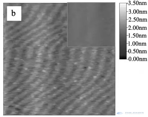
First, use SiO2 mechanical polishing directly. The surface quality is measured by Kla Tencor-10’s Candela with an accuracy of 300nm and the CSPM4000 atomic force microscope (AFM) with an accuracy of 0.01nm. The scratch depth can be measured to be 9.78nm.
The surface oxygen content and penetration depth are analyzed by K-Alpha X-ray photoelectron spectroscopy (XPS) instrument: the standard sample is He+ sputtering standard SiO2 sample, and the sputtering rate is 25nm/min; the sample is He+ sputtering SiC sample. The hardness of SiC is greater than that of SiO2, so the sputtering rate is less than 25nm/min. After sputtering 0.25min, the oxygen signal is zero, so the penetration depth is less than 25nm/min*0.25min=6.25nm. The penetration depth is less than the depth of the scratch, indicating that the scratch is caused by mechanical action, rather than oxidation.
Second, in the same way, if you use hydrogen peroxide to polish directly, scratches will be added. The AFM diagram is shown as follows. The reason is that the chemical corrosion is anisotropic and will accelerate corrosion for crystals with large surface energy.
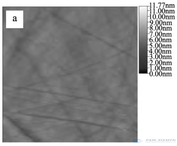
If only immersion in hydrogen peroxide, the defects and scratches will be enlarged. After immersion, the surface roughness of the wafer increased from 0.06nm to 0.14nm. The AFM diagram is shown as follows, and the upper right corner is before soaking:
How to Perform a Typical Chemical Mechanical Polishing on Silicone Carbide?
After knowing that chemical + mechanical polishing is required, the typical chemical mechanical polishing on silicon carbide is as follows:
The first step is mechanical polishing.
Use a 0.5um diameter diamond polishing solution to polish the surface roughness to 0.7nm.
The second step is chemical mechanical polishing.
- Polishing machine: AP-810 single-sided polishing machine;
- Polishing pressure is 200g/cm2;
- Rotation speed of main plate is 50r/min;
- The ceramic disc speed is 38r/min;
- Polishing liquid composition: Based on SiO2 (30wt%, pH=10.15), add 0-70wt% hydrogen peroxide (30wt%, pure premium grade), and finally adjust pH=8.5 with KOH (5wt %) and HNO3 (1wt %);
- The polishing liquid flow rate is 3L/min, and it is recycled.
In fact, various parameters are adjustable, and suitable conditions should be selected for the wafer and the machine:
- Optional mechanical polishing liquid: SiO2, Al2O3, cerium dioxide;
- Optional chemical polishing liquid: potassium permanganate, hydrogen peroxide, Pt catalyst, Fe catalyst;
- Optional polishing pad: nylon, polyurethane;
- Acidity and alkalinity: KOH, HNO3;
- Mechanical action: pressure, speed, position, time, temperature.

For more information, please contact us email at victorchan@powerwaywafer.com and powerwaymaterial@gmail.com.