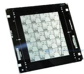
Photomask blank with antireflective chromium is available. Photomasks are mainly used in integrated circuits, flat panel displays (including LCD, LED, OLED), printed circuit boards and other fields. The photomask is a pattern master used in the photolithography process in microelectronics manufacturing. Here are specifications of photo mask blank for your reference:
No. 1 Photo Masks PAM190302-MASKH
No. 1-1 Silicon wafers with IC structures (ASIC11) at 0.35 micron design standards;
No.1-2 Silicon wafers with IC structures (ASIC12) at 0.35 micron design standards;
Note:
The diameter of the substrate >= 150mm. the type / doping admixture, orientation, thickness, resistivity, front surface, rear surface, flat (s) is determined by the manufacturer to provide the required element base parameters (transistors, resistors, capacitors) specified in the Design Kit. The manufacturer provides a Design Kit suitable for IC topology development. The customer performs the development in accordance with the Design Kit and transmits the information to the manufacturer in GDS format. The manufacturer produces a set of photomasks in accordance with the information in the GDS format. The manufacturer manufactures the plates using a set of photomasks and according to the Design Kit requirement.
No. 1-3 Photomask Blank
size 152 x 152 x mm, scale 5: 1, designed for photolithography with design standards of 0.35 μm;
Basic Template Requirements
Purpose: binary templates for projection f / l
Substrate size: 6 “x6” x0.25 “, quartz
Equipment type: 5x, NIKON NSR 2205i11D
Exposure field: 110 mm x 110 mm
Pellicle: Yes, NIK49P-122-1K17 / HFLC, one-side protection from chrome (two-way protection on demand)
Minimum critical size: 1.75 microns
Reproducibility of critical dimensions: 0.05 µm (3σ)
Registration Accuracy (Registration): 0.1 µm
Defect: 0.1 / cm2 (1 micron)
No. 2 Chromium Photomask on Quartz PAM200313-MASKH
No. 2-1 Least complex one: Strip & Ship;
CD >= 5um;
Vast open areas; Write Grid: Standard
Material: quartz, antireflective chromium. No pellicle.
No. 2-2 Moderate one:
5x reticle; 6”x6”x0.12” Quartz;
No defects bigger than 2,5um;
Smaller than 1,25um defect
CD >= 5um; lines/spaces/octagons;
Write Grid: Should maintain CD
Material: quartz, antireflective chromium. No pellicle.
No. 2-3 Most complex one:
5x reticle; 6”x6”x0.12” Quartz;
No defects bigger than 1,25um;
Smaller than 0,625um defect
CD >= 2,5um; lines/spaces/ octagons;
Write Grid: Should maintain CD
Material: quartz, antireflective chromium. No pellicle.
There won’t be any pellicle necessary in these photomask blanks, and the reticle mask size will be 6” x 6” and 0.12” in thickness. Min feature sizes on masks are 2,5um and 5um. Photomask (reticle) is for fabrication of the lithography process to be used in stepper machines.
The technical parameters of photomask blank meet the requirement in Table 1 and Table 2.
|
Table 1 Photo Mask Quality Level Parameters |
||||||||||||||||
| Grade | D | C | B | A | S | T | U | V | W | W+P | X | X+P | Y | Y+P | Z | Z+P |
| Tolerance | ±0.3 | ±0.3 | ±0.2 | ±0.15 | ±0.1 | ±0.1 | ±0.05 | ±0.04 | ±0.035 | ±0.035 | ±0.032 | ±0.032 | ±0.028 | ±0.028 | ±0.022 | ±0.022 |
| Mean to target | ±0.3 | ±0.3 | ±0.2 | ±0.15 | ±0.1 | ±0.075 | ±0.05 | ±0.04 | ±0.03 | ±0.03 | ±0.028 | ±0.028 | ±0.025 | ±0.025 | ±0.02 | ±0.02 |
| Uniformity | 0.2 | 0.2 | 0.2 | 0.15 | 0.1 | 0.075 | 0.05 | 0.04 | 0.035 | 0.035 | 0.035 | 0.035 | 0.03 | 0.03 | 0.025 | 0.025 |
| Registration | ±0.4 | ±0.3 | ±0.2 | ±0.15 | ±0.1 | ±0.075 | ±0.05 | ±0.06 | ±0.055 | ±0.055 | ±0.05 | ±0.05 | ±0.045 | ±0.045 | ±0.04 | ±0.04 |
| Defect size | 1.5 | 1.5 | 1 | 0.8 | 0.6 | 0.4 | 0.4 | 0.35 | 0.3 | 0.3 | 0.25 | 0.25 | 0.2 | 0.2 | 0.2 | 0.2 |
| Defect density | 0 | 0 | 0 | 0 | 0 | 0 | 0 | 0 | 0 | 0 | 0 | 0 | 0 | 0 | 0 | 0 |
| Edge defect | / | / | / | / | / | / | / | 0.3 | 0.3 | 0.3 | 0.25 | 0.25 | 0.2 | 0.2 | 0.2 | 0.2 |
| Edge roughness | / | / | / | / | / | / | / | 0.3 | 0.3 | 0.3 | 0.25 | 0.25 | 0.2 | 0.2 | 0.2 | 0.2 |
| Corner rounding | / | / | / | / | / | / | / | 0.3 | 0.3 | 0.3 | 0.25 | 0.25 | 0.2 | 0.2 | 0.2 | 0.2 |
| PSM phase | / | / | / | / | / | / | / | / | / | 180±4 | / | 180±3 | / | 180±3 | / | 180±3 |
| PSM trans | / | / | / | / | / | / | / | / | / | 6±0.4 | / | 6±0.3 | / | 6±0.3 | / | 6±0.3 |
Note:
The parameters are applicable to scale reticle; the quality level is ranked from low to high:
- 0.5um process supports up to S level; 0.35um process supports up to U level, 0.18um process supports up to X level;
- Ordinary glass mask is only applicable to Class D.
| Table 2 Requirements for Photomask Quality | ||||||||
| 1:1 Main Mask | 1:1 Electron Beam Scanning | UT mask | ||||||
| Grade | PB | PA | EB | EA | ES | uc | UB | UA |
| CD spec | >2.5 | 1.2~2.5 | >1.5 | 1.2~1.5 | <1.2 | >2 | 1.5~2.0 | <1.5 |
| Tolerance | ±0.25 | ±0.2 | ±0.2 | ±0.15 | ±0.1 | ±0.25 | ±0.2 | ±0.15 |
| Uniformity | 0.3 | 0.3 | 0.3 | 0.25 | 0.2 | 0.25 | 0.2 | 0.15 |
| Registration | ±0.8 | ±0.8 | ±0.2 | ±0.15 | ±0.1 | ±0.2 | ±0.15 | ±0.1 |
| Defect size | 2 | 2 | 1.5 | 1.5 | 1.0 | 2 | 1.5 | 1 |
| Defect density(pcs/in2) | 2 | 1 | 2 | 1 | 0.5 | 0 | 0 | 0 |
Note:
The requirement is applicable to 1:1 mask, and the quality level is ranked from low to high;
UT mask is only applicable to quartz material; ordinary glass mask is applicable to the highest level B.
No.3 Photolithography Blank PAM200326-MASKH
Glass substrate:
Size: 50x50mm +/-0.2mm;
Thickness: 3.67mm +/-0.02mm
Material: QUARTZ
No Spec. on Flatness: 1/4 ~ 1/2 wavelength
Free of chip on edges
Starting substrate 7X7inch X 150mil
Standard reticle blank Coating 3.0 OD AR Chrome
No. 4 Photo Mask on Quartz PAM200602-MASKH
No. 4-1 Photo mask
Mask size 5” X5”
MASK SUBSTRATE MATERIALS: Quartz
Lithography: electron beam
Mask polarity: BF
Feature tolerance: 0.02um
Feature size: 0.4um
Accuracy: 0.12 um
Manufacturing Grid: 0.005um, 0.02um
No. 4-2 Photomask Blank
Mask size 5” X5”
MASK SUBSTRATE MATERIALS Quartz
Lithography: laser
Mask polarity: DF
Feature tolerance: 0.5um
Feature size: 10 um, 3um, or 5um
Accuracy: 0.12 um
Manufacturing Grid: 0.02um
No. 5 Quartz with LR Chrome PAM200811-MASKH
Mask size= 5″x 5″x 0.09″
Material = Quartz with LR Chrome
Orientation: RR Down.
Data Dark .
Critical Dimension (CD): 4 µm +/- 0.5 µm (for all masks)
Defects: 0 > 5 µm
Please note:
The Quartz with LR Chrome is for fabricating Mask Aligner (NUV Photo lithography 350-450 nm wavelength);
Data to mask scaling is 1:01 because mask aligner have scaling 1:1, instead of 5:1;
Mask material is Quartz with LR Chrome, and Chrome side is facing down (Real Read (RR) down);
In layout designing, Metal layer number 28 is used, and the area of metal layer in the design layouts should be chrome on the photo mask.

For more information, please contact us email at victorchan@powerwaywafer.com and powerwaymaterial@gmail.com.