
Customized Silicon Carbide Substrate
PAM-XIAMEN can provide Silicon Carbide(SiC) customization to meet the specific needs of research institutions, universities, and enterprises for R&D or mass production. We have rich experience in microfabrication of hard and brittle materials, with processing capabilities such as cutting, polishing, thinning, slicing, and coating, which can meet the performance requirements of your device design with custom-made SiC wafer. If you need customized silicon carbide wafer, please contact us at [email protected] immediately to discuss your requirements with our engineers.
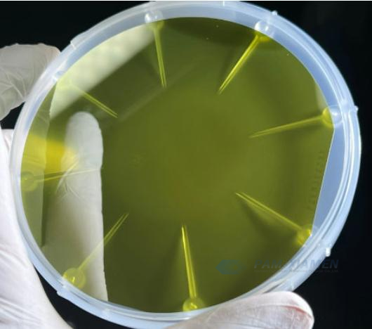
1. Specifications of Customized Silicon Carbide Substrate
Size: 2, 3, 4, 6, 8 inches and other square sizes
Crystal polytype: 4H
Crystal orientation: (0001) orientation on-axis or 4° off-axis
Conductive type: N-type, P-type, semi-insulating
Customized thickness: 100um~2000um
1.1 As-Cut SiC Substrate
We are proficient in cutting techniques, such as diamond wire cutting, mortar wire cutting, laser cutting for silicon carbide crystals.
SiC as-cut wafers are widely used in the processing and testing of silicon carbide materials for subsequent grinding and polishing equipment.
1.2 Polished SiC Substrate
Surface finished: double-side CMP, or C-surface polished/Si surface CMP
Polishing process: Proficient in mechanical polishing, chemical polishing, chemical mechanical polishing and other polishing techniques
Surface roughness: Min. Ra< 0.2nm
Max. Ra<5nm
1.3 Customized Silicon Carbide Wafer in Sizes
Dimensions: 10 * 10mm, 20 * 20mm, etc.
Scribing process: Proficient in mastering grinding wheel cutting, laser full cutting, laser half cutting, laser invisible cutting, and water guided laser cutting. Among them, the processing method combining laser invisible scribing and fragmentation has high processing efficiency and meets production requirements.
1.4 SiC Thinning Wafer
Min. Thickness: 100um
Processing: single-sided thinning; double-sided thinning
Process: Proficient in thinning techniques such as mechanical grinding and chemical mechanical polishing
2. SiC Substrate Coating
Coating is a commonly used surface treatment process, which generally involves depositing a certain metal or non-metal in vapor phase on the surface of a material in a vacuum environment, forming a dense thin film. The quality of coating is crucial for the functional formation of semiconductor devices, and the materials can be metal materials, semiconductor materials, and compound materials such as oxide fluorides.
PAM-XIAMEN has mastered various SiC coating technologies such as electron beam evaporation, magnetron sputtering, LPCVD, PECVD, atomic layer deposition, etc., and can perform coating according to demands in our silicon carbide foundry:
Wafer Size: 2, 3, 4, 6, 8 inches
Coating thickness: nm level, um level, can be customized according to needs
Coating surface: single-sided or double-sided
Coating layers: single-layer or multi-layers
2.1 Metal Film for SiC
PAM-XIAMEN can process metals such as Ni, Ti, Cu, Au, Pt, Al, Mo, Ni, Ag, W, Ta, Pd, Cr, etc.
Tell us your specific applications, we will provide you with professional advice on custom silicon carbide coating solutions.
2.2 Optical Coating for SiC
Optical coating mainly involves depositing one or more thin films with specific optical properties on the SiC surface to control the reflection, transmission, absorption, and scattering of light. These films alter their optical properties through interference, absorption, and scattering effects. PAM-XIAMEN mainly coat SiC substrate with:
- Anti-Reflective (AR) Coating
- Enhancement Coating
2.3 Si3N4 Coating on Silicon Carbide
Si3N4 coatings deposited by LPCVD and PECVD have their own advantages and applicable fields. The method for Si3N4 deposition mainly depends on specific application and process requirements.

Whether you need high-quality customize silicon carbide (SiC) substrates for research or for industrial applications, please contact us email at [email protected] and [email protected].