Single crystal diamond for sale from PAM-XIAMEN is grown by chemical vapor deposition (CVD), which is a method of decomposing hydrogen and hydrocarbon gas into hydrocarbon active groups at high temperature, and depositing diamond on the substrate material under certain conditions. Theoretically, the method is unlimited in size. Moreover, the prepared electronic level single crystal diamond is of high quality, can be completely colorless and transparent, and has almost no impurities. At the same time, if the doping gas is selectively introduced during the CVD single crystal diamond growth process, a variety of colored diamonds can be prepared. Because there are many advantages of CVD diamond, the diamond wafers become the main material for high power electronics and cutting-edge fields, such as communications, energy, semiconductors, and aerospace.
More about the growth process of diamond substrate, please watch the video: https://youtu.be/XQEFCeY06Do.
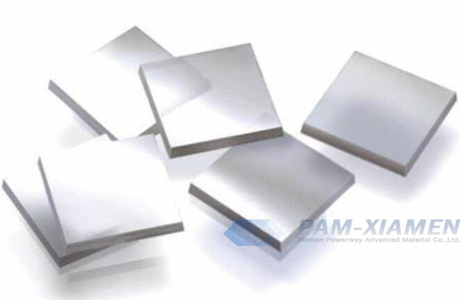
1. Specifications of Single Crystal Diamond Wafer
PAM-210819-DIAMOND
| Item | Single Crystal CVD Diamond Wafer |
| Size | 3x3mm2, 7x7mm2 |
| Orientation | (100)+/-2deg |
| Thickness | 200um+/-25um |
| Half peak width of rocking curve | <=55arcsec |
| Transmittance at 270nm of UV-Vis spectrum | > 50% |
| Raman half peak width | <=2.8cm |
| Plane parallelism | < 20um |
| Surface roughness | < 2nm |
| Surface process | Double side polished |
2. Diamond Material Characteristics
Diamond is an ultra-wide bandgap semiconductor material with a band gap of 5.5 eV, which is larger than wide band gap semiconductor materials such as GaN and SiC. As shown in the table below, the diamond band gap is 5 times that of Si; the carrier mobility is also 3 times that of Si material. Theoretically, the carrier mobility of diamond is higher than that of existing wide-bandgap semiconductor materials (GaN, SiC). It is also more than 2 times higher. Meanwhile, diamond has a very low intrinsic carrier concentration at room temperature. Moreover, in addition to the highest hardness, single crystal diamond thermal conductivity is the highest one among semiconductor materials, which is 7.5 times that of AlN. Based on these excellent performance parameters, single crystal of diamond is considered to be the most promising material for the preparation of next-generation high-power, high-frequency, high-temperature and low-power loss electronic devices.
| Material | Bandgap Width eV | Intrinsic Carrier Concentration cm-3 | Electron Mobility cm2/Vs | Electron Saturation Velocity 107cm/s | Breakdown Field Strength MV/cm | Thermal Conductivity W/cmK |
| Diamond | 5.47 | ~10-27 | 4500 | 1.5 | >20 | 22 |
| AlN | 6.2 | ~10-31 | 1100 | 2.2 | 12 | 2.9 |
| Gallium Oxide | 4.8-5.0 | ~10-22 | 300 | – | 8 | 0.11/0.27 |
| GaN | 3.4 | ~10-10 | 2000 | 2.5 | 3.2 | 1.3 |
| SiC | 3.3 | ~10-9 | 950 | 2.0 | 3.0 | 4.9 |
| GaAs | 1.4 | 106 | 8500 | 2.0 | 0.4 | 0.43 |
| Si | 1.1 | 1010 | 1500 | 1.0 | 0.3 | 1.5 |
3. CVD Single Crystal Diamond Substrate Application in Semiconductor
The remarkable progress of single crystal diamond growth by chemical vapor deposition makes it possible to prepare diamond suitable for radiation detection on a conventional basis. With the continuous improvement of CVD method, it is possible to grow a large-area homoepitaxial single crystal CVD diamond plate / film. Single crystal diamond CVD wafer has broad application prospects, such as radio frequency diodes, bipolar junction transistors, field effect transistors, micro-electromechanical systems (MEMS) and electronics industry.
Due to the high atomic density of diamond, it is difficult to dope and conduct electricity, so the field effect transistor is mainly produced by hydrogen terminal surface conductance. However, the characteristics of diamond are very good. MoO3 is introduced, which is a transfer doping medium, under the gate of the hydrogen-terminated diamond field effect transistor. The forward conduction resistance is reduced to 1/3 of that of the MOSFET based on EL SC diamond wafer with the same gate length, and the transconductance is increased by approximately 3 times.
Single -crystal diamond wafers have made great progress in the power electronics in electrical vehicles and RF power technology for satellites and 5G communications.
In particular, the era of 5G communication is rapidly and comprehensively, and the application of single crystal bulk diamond in semiconductors and high-frequency power devices has become increasingly prominent. The single crystal diamond for large size are an important material foundation for the implementation of major national strategies such as ultra-precision processing and smart grid, as well as the upgrading of industrial clusters such as smart manufacturing and 5G communications. For this reason, the research of diamond materials is required to develop in the direction of large size, low defects, low resistivity and high thermal conductivity.

For more information, please contact us email at victorchan@powerwaywafer.com and powerwaymaterial@gmail.com.