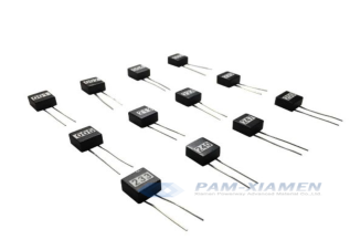
PAM XIAMEN offers 3″ Silicon Wafer.
Diameter
Type
Dopant
Growth
method
Orientation
Resistivity
Thickness
Surface
Grade
76.2
P
Boron
CZ
-100
.001-.005
350-400
P/E
PRIME
76.2
P
Boron
CZ
-100
.005-.02
350-400
P/E
PRIME
76.2
P
Boron
FZ
-100
>3000
350-400
P/E
PRIME
76.2
P
Boron
CZ
-100
1-20
350-400
P/E
PRIME
76.2
P
Boron
CZ
-100
1-20
350-400
P/E/DTOx
PRIME
76.2
P
Boron
CZ
-100
1-20
350-400
P/E/Ni
PRIME
76.2
P
Boron
CZ
-100
1-20
350-400
P/E/WTOx
76.2
P
Boron
CZ
-100
1-20
450-500
P/P
PRIME
76.2
P
Boron
CZ
-100
1-20
500-550
P/E
PRIME
76.2
P
Boron
CZ
-100
1-10
825-875
P/P
PRIME
76.2
P
Boron
CZ
-100
1-20
850-1000
P/P
PRIME
76.2
P
Boron
CZ
-100
1-20
1000-1050
P/E
PRIME
76.2
P
Boron
CZ
-111
1-20
300-350
P/P
PRIME
76.2
P
Boron
CZ
-111
1-20
350-400
P/E
PRIME
76.2
P
Boron
CZ
-110
>100
275-325
P/P
PRIME
76.2
P
Boron
CZ
-110
1-20
350-400
P/E
PRIME
76.2
P
Boron
CZ
-110
100-200
800-850
P/P
PRIME
76.2
Any
Any
CZ
Any
Any
250-500
P/E
TEST
76.2
Any
Any
CZ
-100
1-100
330-430
P/E
PRIME
76.2
Intrinsic
Undoped
FZ
-100
> 15000
350-400
P/E
PRIME
76.2
Intrinsic
Undoped
FZ
-111
> 15000
350-400
P/E
PRIME
For more information, please visit our website: https://www.powerwaywafer.com,
send us email at sales@powerwaywafer.com and powerwaymaterial@gmail.com
Found in 1990, Xiamen Powerway Advanced Material Co., Ltd (PAM-XIAMEN) is a leading manufacturer of semiconductor material in China.PAM-XIAMEN develops advanced crystal growth and [...]
2019-03-04meta-author
PAM XIAMEN offers Single Crystal Quartz Wafers.
All single crystal quartz should be grown from one special seed.
And the different cut type will cause the different seed location.
One type is inside the wafer names “with seed”, the other type is not inside the wafers, so [...]
2019-02-27meta-author
White light emission of monolithic InGaN/GaN grown on morphology-controlled, nanostructured GaN templates
We demonstrated an InGaN/GaN-based, monolithic, white light-emitting diode (LED) without phosphors by using morphology-controlled active layers formed on multi-facet GaN templates containing polar and semipolar surfaces. The nanostructured surface morphology was controlled by [...]
2018-07-12meta-author
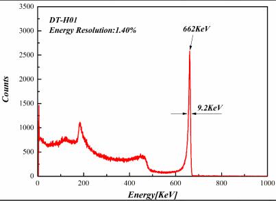
PAM-PA03 series are pixel electrode structured detectors based on CZT crystal.
1. CZT Compton Imaging Detector Specification
Material
CdZnTe
Density
5.8g/cm3
Volume resistivity
>1010Ω.cm
Dimension
22.0×22.0 mm2
Thickness
15.0mm
Pixel size
1.38×1.38 mm2
Pixel center space
1.88mm
Pixel array
11×11
Electrode material
Au
Operation temperature
25℃-+40℃
Energy range
60KeV~2.6MeV
Energy resolution(22℃)
Average pixel <5%@662KeV
Storage temperture
10℃~40℃
Storage humidity
20%-80%
2. Spectrum of CZT Compton Imager
3. Features Compton Imaging Detector Based on CZT Crystal
Long-time stability
High energy [...]
2019-04-24meta-author
PAM-XIAMEN can offered SiC wafers, specific specifications and parameters can be found in: https://www.powerwaywafer.com/sic-wafer
4H-SiC single crystal has excellent characteristics such as wide bandgap, high carrier mobility, high thermal conductivity, and good stability. It has broad application prospects in high-power electronics, radio frequency/microwave electronics, and quantum information. [...]
2024-03-15meta-author
PAM-XIAMEN can offer 2&3 inches P-type GaAs substrates. Gallium arsenide (GaAs) is a III-V type direct band gap semiconductor with a zinc blend crystal structure, and GaAs p-type dopant is commonly used as a substrate for epitaxial growth of other III-V semiconductors, including indium gallium arsenide, aluminum gallium [...]
2021-04-15meta-author