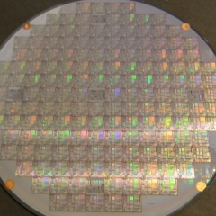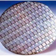
GaAs (galliumarsenid) Wafers
As a leading GaAs substrate supplier, PAM-XIAMEN manufactures Epi-ready GaAs(Gallium Arsenide) Wafer Substrate including semi-conducting n type, semi-conductor C doped and p type with prime grade and dummy grade. The GaAs substrate resistivity depends on dopants, Si doped or Zn doped is (0.001~0.009) ohm.cm, C doped one is >=1E7 ohm.cm. The GaAs wafer crystal orientation should be (100) and (111). For (100) orientation, it can be 2°/6°/15° off. The EPD of GaAs wafer normally is <5000/cm2 for LED or <500/cm2 for LD or microelectronics.
- Beskrivelse
Beskrivelse
(galliumarsenid) GaAs Wafer
PAM-XIAMEN udvikler og producerer sammensatte halvledersubstrater - galliumarsenidkrystal og wafer. Vi har brugt avanceret krystalvækstteknologi, vertikal gradientfrysning (VGF) og GaAs-wafer-fremstillingsproces, etableret en produktionslinje fra krystalvækst, skæring, slibning til poleringsbearbejdning og bygget et 100-klasses rent rum til GaAs wafer-rensning og -pakning. Vores GaAs-wafere inkluderer 2~6 tommer ingot/wafers til LED-, LD- og Microelectronics-applikationer. Vi er altid dedikerede til at forbedre kvaliteten af nuværende GaAs wafer substrater og udvikle store størrelse substrater. Den tilbudte GaAs-waferstørrelse er i 2”, 3”, 4” og 6”, og tykkelsen skal være 220-700um. Desuden er GaAs wafer-prisen fra os konkurrencedygtig.
1. GaAs Wafer Specifikationer
1.1 (GaAs)galliumarsenidVafler til LED-applikationer
| Vare | Specifikationer | Bemærkninger |
| varmeledning type | SC / n-type | SC / p-typen med Zn dope Tilgængelig |
| vækst Metode | VGF | |
| dopingmiddel | Silicon | Zn tilgængelig |
| wafer i diameter | 2, 3 & 4 inch | Barre eller som-cut availalbe |
| Crystal Orientering | (100) 2 °/ 6 ° / 15 ° off (110) | Andre misorientation tilgængelig |
| AF | EJ eller USA | |
| Carrier Koncentration | (0,4 ~ 2,5) E18 / cm3 | |
| Resistivity ved RT | (1,5 ~ 9) E-3 Ohm.cm | |
| Mobilitet | 1500 ~ 3000cm2 / V-sek | |
| Etch Pit Density | <5000 / cm2 | |
| Laser Mærkning | efter anmodning | |
| Surface Finish | P / E eller P / P | |
| Tykkelse | 220 ~ 450um | |
| epitaksi Ready | Ja | |
| Pakke | Enkelt wafer beholder eller kassette | |
1.2 (GaAs)galliumarsenidVafler til LD Applications
| Vare | Specifikationer | Bemærkninger |
| varmeledning type | SC / n-type | |
| vækst Metode | VGF | |
| dopingmiddel | Silicon | |
| wafer i diameter | 2, 3 & 4 inch | Barre eller som-cut rådighed |
| Crystal Orientering | (100) 2 °/ 6 ° / 15 ° off (110) | Andre misorientation tilgængelig |
| AF | EJ eller USA | |
| Carrier Koncentration | (0,4 ~ 2,5) E18 / cm3 | |
| Resistivity ved RT | (1,5 ~ 9) E-3 Ohm.cm | |
| Mobilitet | 1500 ~ 3000 cm2 / V-sek | |
| Etch Pit Density | <500 / cm2 | |
| Laser Mærkning | efter anmodning | |
| Surface Finish | P / E eller P / P | |
| Tykkelse | 220 ~ 350um | |
| epitaksi Ready | Ja | |
| Pakke | Enkelt wafer beholder eller kassette | |
1,3 (GaAs)galliumarsenidWafers, Semi-isolerende for Microelectronics Applications
| Vare | Specifikationer | Bemærkninger |
| varmeledning type | isolerende | |
| vækst Metode | VGF | |
| dopingmiddel | C doped | |
| wafer i diameter | 2, 3 & 4 inch | Ingot tilgængelig |
| Crystal Orientering | (100)+/- 0,5° | |
| AF | EJ, USA eller hak | |
| Carrier Koncentration | n / a | |
| Resistivity ved RT | > 1E7 Ohm.cm | |
| Mobilitet | > 5000 cm2 / V-sek | |
| Etch Pit Density | <8000 / cm2 | |
| Laser Mærkning | efter anmodning | |
| Surface Finish | P / P | |
| Tykkelse | 350 ~ 675um | |
| epitaksi Ready | Ja | |
| Pakke | Enkelt wafer beholder eller kassette | |
1,4 6" (150 mm) (GaAs)galliumarsenidWafers, Semi-isolerende for Microelectronics Applications
| Vare | Specifikationer | Bemærkninger |
| varmeledning type | Semi-isolerende | - |
| Grow Metode | VGF | - |
| dopingmiddel | C doped | - |
| Type | N | - |
| Elektrodens diameter (mm) | 150 ± 0,25 | - |
| Orientering | (100)0°±3,0° | - |
| HAK Orientering | 〔010〕 ± 2 ° | - |
| NOTCH deepth (mm) | (1-1,25)mm 89°-95° | - |
| Carrier Koncentration | kontakt venligst vores salgsteam | - |
| Resistivity (ohm.cm) | >1,0×10⁷ | - |
| Mobilitet (cm2 / vs) | kontakt venligst vores salgsteam | - |
| forvridning | kontakt venligst vores salgsteam | - |
| Tykkelse (um) | 675 ± 25 | - |
| Edge Udelukkelse for Bow og Warp (mm) | kontakt venligst vores salgsteam | - |
| Bow (um) | kontakt venligst vores salgsteam | - |
| Warp (um) | ≤20.0 | - |
| TTV (um) | ≤10.0 | - |
| TIR (um) | ≤10.0 | - |
| LFPD (um) | kontakt venligst vores salgsteam | - |
| Polering | P / P Epi-Ready | - |
1,5 2" (50,8 mm) LT-GaAs (Lav temperatur-Grown Galium arsenid) Wafer Specifikationer
| Vare | Specifikationer |
| varmeledning type | Semi-isolerende |
| Grow Metode | VGF |
| dopingmiddel | Sub:C doped / Epi:Undoped |
| Type | N |
| Elektrodens diameter (mm) | 150 ± 0,25 |
| Orientering | (100)0°±3,0° |
| HAK Orientering | 〔010〕 ± 2 ° |
| NOTCH deepth (mm) | (1-1,25)mm 89°-95° |
| Carrier Koncentration | kontakt venligst vores salgsteam |
| Resistivity (ohm.cm) | >1,0×10⁷ eller 0,8-9 x10⁻³ |
| Mobilitet (cm2 / vs) | kontakt venligst vores salgsteam |
| forvridning | kontakt venligst vores salgsteam |
| Tykkelse (um) | 675 ± 25 |
| Edge Udelukkelse for Bow og Warp (mm) | kontakt venligst vores salgsteam |
| Bow (um) | kontakt venligst vores salgsteam |
| Warp (um) | ≤20.0 |
| TTV (um) | ≤10.0 |
| TIR (um) | ≤10.0 |
| LFPD (um) | kontakt venligst vores salgsteam |
| Polering | P / P Epi-Ready |
2. GaAs Wafer Market & Application
Galliumarsenid er et vigtigt halvledermateriale. Det tilhører gruppe III-V sammensatte halvledere og zinkblandede krystalgitterstrukturen med en gitterkonstant på 5,65×10⁻¹⁰m, et smeltepunkt på 1237°C og et båndgab på 1,4 elektronvolt. Galliumarsenid kan laves til semi-isolerende højmodstandsmaterialer, som kan bruges til at fremstille integrerede kredsløbssubstrater, infrarøde detektorer, gammafotondetektorer osv. Fordi dets elektronmobilitet er 5 til 6 gange større end silicium, har SI GaAs-substratet været vigtigt brugt i fremstillingen af mikrobølgeenheder og højhastigheds digitale kredsløb. Halvlederenheder fremstillet på galliumarsenid har fordelene ved høj frekvens, høj temperatur, lav temperatur ydeevne, lav støj og stærk strålingsmodstand, hvilket får GaAs substratmarkedet til at udvide.
3. Testcertifikat for GaAs-wafer kan omfatte nedenstående analyse, hvis det er nødvendigt:
1/Overfladeruhed af galliumarsenid inklusive forside og bagside (nanometer).
2/Dopingkoncentration af galliumarsenid(cm-3)
3/EPD af galliumarsenid(cm-2)
4/Mobility of Gallium Arsendie(V.sec)
5/Røntgendiffraktionsanalyse (rokkekurver) af galliumarsenid: Diffraktionsreflektionskurve halv bredde
6/Lavtemperaturfotoluminescens (emissionsspektre i området 0,7-1,0 μm) af galliumarsenid: Fraktionen af excitonfotoluminescens i emissionsspektret af nær-IR-området ved en temperatur på 4K eller 5 K og en optisk excitationstæthed på 1 W/cm2
7/Transmissionshastighed eller Absorptionskoefficient: For et øjeblik kan vi måle absorptionskoefficienten for enkeltkrystal udopede GaAs ved 1064nm: <0,6423 cm-1, og dette svarer til et transmissionsminimum på 33,2% for et nøjagtigt 6,5 mm tykt emne ved 1064nm.
Bemærkning:
Den kinesiske regering har annonceret nye grænser for eksport af galliummaterialer (såsom GaAs, GaN, Ga2O3, GaP, InGaAs og GaSb) og germaniummaterialer, der bruges til at fremstille halvlederchips. Fra den 1. august 2023 er eksport af disse materialer kun tilladt, hvis vi opnår en licens fra det kinesiske handelsministerium. Håber på jeres forståelse og samarbejde!
Du kan også gerne ...
-
Nanofabrikationsfotoresist
PAM-XIAMEN Tilbud fotoresist plade med fotoresist
-
SiC Wafer Substrat
Virksomheden har en komplet SiC(siliciumcarbid) wafersubstratproduktionslinje, der integrerer krystalvækst, krystalbehandling, waferbehandling, polering, rensning og testning. I dag leverer vi kommercielle 4H og 6H SiC wafere med semi-isolering og ledningsevne i on-axis eller off-axis, tilgængelige størrelser: 5x5mm2,10x10mm2, 2",3",4", 6" og 8", der bryder igennem nøgleteknologier som f.eks. som defektundertrykkelse, frøkrystalbehandling og hurtig vækst, fremme af grundlæggende forskning og udvikling relateret til siliciumcarbidepitaksi, enheder mv.
-
Float-Zone Mono-krystallinsk silicium
PAM-XIAMEN kan tilbyde float zone silicium wafer, som opnås ved Float Zone metoden. Monokrystallinske siliciumstænger føres gennem floatzonevækst, og forarbejde derefter de monokrystallinske siliciumstænger til siliciumwafers, kaldet floatzone siliciumwafers. Da den zonesmeltede siliciumwafer ikke er i kontakt med kvartsdigelen under den flydende zone siliciumproces, er siliciummaterialet i en suspenderet tilstand. Derved er det mindre forurenet under processen med flydende zonesmeltning af silicium. Kulstofindholdet og oxygenindholdet er lavere, urenhederne er mindre, og resistiviteten er højere. Den er velegnet til fremstilling af strømudstyr og visse elektroniske højspændingsenheder.
-
GaAs Epiwafer
PAM-XIAMEN fremstiller forskellige typer epi wafer III-V siliciumdoteret n-type halvledermaterialer baseret på Ga, Al, In, As og P dyrket af MBE eller MOCVD. Vi leverer tilpassede GaAs epiwafer-strukturer for at opfylde kundernes specifikationer, kontakt os venligst for mere information.
-
Ge (Germanium) enkelte krystaller og Wafers
PAM-XIAMEN tilbyder 2”, 3”, 4” og 6” germanium wafer, som er en forkortelse for Ge wafer dyrket af VGF / LEC. Let dopet P- og N-type Germanium-wafer kan også bruges til Hall-effekteksperiment. Ved stuetemperatur er krystallinsk germanium skørt og har ringe plasticitet. Germanium har halvlederegenskaber. Germanium med høj renhed er dopet med trivalente grundstoffer (såsom indium, gallium, bor) for at opnå P-type germanium-halvledere; og pentavalente grundstoffer (såsom antimon, arsen og phosphor) doperes for at opnå N-type germanium-halvledere. Germanium har gode halvlederegenskaber, såsom høj elektronmobilitet og høj hulmobilitet. -
CdZnTe (CdZnTe) Wafer
Cadmium (CdZnTe eller CdZnTe) er en ny halvleder, som gør det muligt at konvertere stråling til elektron effektivt er den hovedsagelig anvendes i infrarødt tyndfilm-epitaxi substrat, X-ray detektorer og Gamma-ray CdZnTe-detektorer. -
InP wafer
PAM-XIAMEN offers VGF InP(Indium Phosphide) wafer with prime or test grade including low dope, N type or semi-insulating. The mobility of InP wafer is different in different type, low doped one>=3000cm2/V.s, N type>1000 or 2000cm2V.s(depends on different doping concentration), P type: 60+/-10 or 80+/-10cm2/V.s(depends on different Zn doping concentration), and semi-insulting one>2000cm2/V.s, the EPD of Indium Phosphide is below 500/cm2 normally.
-
Fritstående GaN-substrat
PAM-XIAMEN har etableret den fremstillingsteknologi til fritstående (galliumnitrid) GaN substratwafer, der er til UHB-LED og LD. Vokset med hydrid dampfase epitaxy (HVPE) teknologi, Vores GaN substrat har lav defekt tæthed.