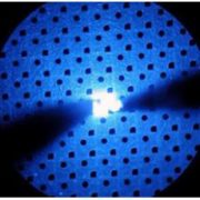
GaN HEMT Epitaxial Wafer
Gallium Nitride (GaN) HEMT'er (High Electron Mobility Transistors) er den næste generation af RF-effekttransistorteknologi. Takket være GaN-teknologien tilbyder PAM-XIAMEN nu AlGaN/GaN HEMT Epi Wafer på safir eller silicium, og AlGaN/GaN på safirskabelon.
- Beskrivelse
Beskrivelse
GaN HEMT epitaksial wafer er en flerlagsfilm dyrket epitaksialt på et substrat, som sædvanligvis omfatter et nukleationslag, et overgangslag, et bufferlag, et kanallag, et barrierelag, et dæklag og et passiveringslag fra bund til top. Kernedannelseslaget, som AlGaN eller AlN, bruges til at forhindre substratmaterialet i at diffundere ind i GaN-epitaksiallaget. Overgangslaget kan indeholde hierarkisk AlGaN, AlN/GaN supergitter eller flerlags AlN for at balancere spændingen mellem GaN og substratet. Jo højere Al-indhold i barrierelaget af AlGaN, jo højere er 2DEG-koncentrationen ved heterojunction. I mellemtiden, jo lavere enhedens tærskelspænding er, og jo højere strømkapacitet. Efterhånden som Al-forholdet stiger, vil graden af heterogen krystalgittermismatch være højere, hvilket resulterer i et fald i galliumnitrid HEMT-elektronmobilitet og et fald i strømkapacitet.
High Electron Mobility Transistor (HEMT) er udviklet baseret på GaN med unik heterostruktur og todimensionel elektrongas. GaN HEMT-fordelene omfatter høj nedbrydningsstyrke, lav on-modstand og hurtigere. Omskiftningshastigheden, som er meget velegnet til mellem- og lavspændingssystemer og mellemstore og små strømsystemer, såsom rejseadaptere, trådløse opladere, AC-DC-konvertere, smart home apparater osv. Den epitaksiale wafer med HEMT-struktur er mere attraktiv i øjeblikket for højfrekvensomformere, hvor GaN HEMT-nedbrydningsspændingen er 600~650 V. Med den hurtige udvikling af galliumnitrid HEMT epi-teknologi vil prisen på GaN HEMT-enheder være konkurrencedygtig, hvilket kan vinde et stort GaN HEMT-marked for GaN HEMT-producenter. På grund af galliumnitrid HEMT-pålideligheden kan det desuden bruges i vid udstrækning inden for industrielle områder, såsom fotovoltaiske invertere, energilagringssystemer og elektriske køretøjer.
1. GaN HEMT Materiale: Tilgængelig størrelse: 2",4",6",8":
Mere specifikke parametre for galliumnitrid HEMT wafer til D-mode GaN HEMT'er, E-mode GaN HEMT'er, GaN HEMT effektforstærker og RF, se venligst:
Vi er eksperter i HEMT struktur, vi tilbyder også GaN HEMT epi wafer i mange år.
For siliciumsubstrat skal vi vide, om du dyrker GaN HEMT på silicium til POWER eller RF, det er anderledes. Ved behov, kontakt venligstvictorchan@powerwaywafer.comfor detaljer.
Til SiC bør du bruge semi-isolerende.
Eller du kan købe AlGaN/GaN HEMT struktur på disse tre strukturer fra os.
2. Nu viser vi dig et eksempel som følger:
2.1 2 ″ (50,8 mm) GaN HEMT Epitaxial Wafers
Vi tilbyder 2″ (50,8 mm) galliumnitrid HEMT wafers, GaN HEMT-strukturen er som følger:
Struktur (fra top til bund):
* udodet GaN-dæksel (2 ~ 3nm)
AlxGa1-xN (18 ~ 40 nm)
AlN (pufferlag)
ikke-doteret GaN (2 ~ 3um)
Safirunderlag
* Vi kan bruge Si3N til at erstatte GaN på toppen, vedhæftningen er stærk, den er belagt med sputter eller PECVD.
2.2 AlGaN/GaN HEMT Epi Wafer på safir/GaN
| Lag # | Sammensætning | Tykkelse | X | dopingmiddel | Transportørkoncentration |
| 5 | GAN | 2 nm | – | – | – |
| 4 | AlxGa1-xN | 8 nm | 0.26 | – | – |
| 3 | AlN | 1 nm | Un-doped | ||
| 2 | GAN | ≥1000 nm | Un-doped | ||
| 1 | Buffer / overgangslag | – | – | ||
| substrat | Silicon | 350 um / 625μm | – | ||
2,3 2" (50,8 mm), 4" (100 mm) AlGaN/GaN HEMT Epi Wafer på Si
2.3.1 Specifikationer for aluminium galliumnitrid (AlGaN) / galliumnitrid (GAN) HEMT (High Electron Mobility Transistor) på siliciumunderlag.
| Krav | Specifikation |
| AlGaN / GaN HEMT Epi Wafer på Si | |
| AlGaN / GaN HEMT-struktur | Se 1.2 |
| substrat Materiale | Silicon |
| Orientering | <111> |
| Vækstmetode | Float Zone |
| varmeledning type | P eller N |
| Størrelse (tomme) | 2” , 4” |
| Tykkelse (um) | 625 |
| bagside | Ru |
| Specifik modstand (Ω-cm) | >6000 |
| Bow (um) | ≤ ± 35 |
2.3.2 Epi-struktur: Revnefri epilag
| Lag # | Sammensætning | Tykkelse | X | dopingmiddel | Transportørkoncentration |
| 5 | GAN | 2 nm | – | – | – |
| 4 | AlxGa1-xN | 8 nm | 0.26 | – | – |
| 3 | AlN | 1 nm | Un-doped | ||
| 2 | GAN | ≥1000 nm | Un-doped | ||
| 1 | Buffer / overgangslag | – | – | ||
| substrat | Silicon | 350 um / 625μm | – | ||
2.3.3 Elektriske egenskaber for AlGaN/GaN HEMT-strukturen
2DEG-mobilitet (ved 300 K): ≥1 800 cm2 / Vs
2DEG arkbærertæthed (ved 300 K): ≥0,9 × 1013 cm-2
RMS Roughness (AFM): ≤ 0,5 nm (5,0 um × 5,0 um scanningsområde)
2,4 2" (50,8 mm) AlGaN/GaN på safir
For specifikation af AlGaN / GaN på safirskabelon, bedes du kontakte vores salgsafdeling: sales@powerwaywafer.com.
GaN HEMT-applikationer:Anvendes i blå laserdioder, ultraviolette lysdioder (ned til 250 nm) og AlGaN/GaN HEMTs enhed.
3. Forklaring af AlGaN/Al/GaN HEMT'er:
Nitride HEMT'er udvikles intensivt til højeffektelektronik i højfrekvensforstærkning og strømafbrydelsesapplikationer. Ofte tabes høj ydeevne i DC-drift, når HEMT skiftes - for eksempel kollapser strømmen, når gatesignalet pulses. Det menes, at sådanne effekter er relateret til ladningsfangning, der maskerer portens virkning på strømmen. Feltplader på kilde- og portelektroderne er blevet brugt til at manipulere det elektriske felt i enheden, hvilket mindsker sådanne fænomener med strøm-sammenbrud.
4. GaN EpitaxialTechnology — Tilpasset GaN-epitaksi på SiC-, Si- og Sapphire-substrat til HEMT'er, LED'er:
GAN HEMT epitaxiale wafers (GAN EPI-wafers)
PAM XIAMEN tilbyder epitaksial vækst af AlGaN/GaN baseret HEMT på Si wafers
5. GaN-enhed:
GaN HEMT
6. Testkarakteriseringsudstyr:
Modstand uden kontakt
Kortlægning af laser tynd filmtykkelse
Bias i høj temperatur / høj luftfugtighed
Termisk stød
DIC Nomarski mikroskop
Atomic Force Microscope (AFM)
Surface Defectivity Scan
Bias i høj temp
4PP Sheets Resistance
Kontaktløs hallmobilitet
Temperaturcyklus
Røntgendiffraktion (XRD) / Reflektans (XRR)
Ellipsometer tykkelse
profilometer
CV-tester
7. Støberifremstilling:
vi tilbyder også støberiGaN HEMTfremstilling i følgende proces:
MOCVD Epitaxy
Metal sputtering / E-Beam
Tørt / vådt metal / dielektrisk ætsning
Tynd film PECVD / LPCVD / Sputtering
RTA / Furnace Annealing
Fotolitografi (0,35um min. CD)
Ionimplantation
Bemærkning:
Den kinesiske regering har annonceret nye grænser for eksport af galliummaterialer (såsom GaAs, GaN, Ga2O3, GaP, InGaAs og GaSb) og germaniummaterialer, der bruges til at fremstille halvlederchips. Fra den 1. august 2023 er eksport af disse materialer kun tilladt, hvis vi opnår en licens fra det kinesiske handelsministerium. Håber på jeres forståelse og samarbejde!
Flere fremstillingstjenester, besøg venligst:GaN Fabrication Services til HEMT-enheder
Gallium arsenid epi wafer af aluminium
650V GaN FET-chip til hurtig opladning
GaN MOSFET-struktur:
GaN MOSFET-struktur på SiC-substrat
Læs mere om GaN HEMT-strukturer:
Du kan også gerne ...
-
SiC Wafer Substrat
Virksomheden har en komplet SiC(siliciumcarbid) wafersubstratproduktionslinje, der integrerer krystalvækst, krystalbehandling, waferbehandling, polering, rensning og testning. I dag leverer vi kommercielle 4H og 6H SiC wafere med semi-isolering og ledningsevne i on-axis eller off-axis, tilgængelige størrelser: 5x5mm2,10x10mm2, 2",3",4", 6" og 8", der bryder igennem nøgleteknologier som f.eks. som defektundertrykkelse, frøkrystalbehandling og hurtig vækst, fremme af grundlæggende forskning og udvikling relateret til siliciumcarbidepitaksi, enheder mv.
-
GASB Wafer
PAM-XIAMEN tilbyder Compound Semiconductor GaSb wafer – galliumantimonid, som dyrkes af LEC(Liquid Encapsulated Czochralski) som epi-ready eller mekanisk kvalitet med n-type, p-type eller semi-isolerende i forskellig orientering(111) eller (100).
-
Ge (Germanium) enkelte krystaller og Wafers
PAM-XIAMEN tilbyder 2”, 3”, 4” og 6” germanium wafer, som er en forkortelse for Ge wafer dyrket af VGF / LEC. Let dopet P- og N-type Germanium-wafer kan også bruges til Hall-effekteksperiment. Ved stuetemperatur er krystallinsk germanium skørt og har ringe plasticitet. Germanium har halvlederegenskaber. Germanium med høj renhed er dopet med trivalente grundstoffer (såsom indium, gallium, bor) for at opnå P-type germanium-halvledere; og pentavalente grundstoffer (såsom antimon, arsen og phosphor) doperes for at opnå N-type germanium-halvledere. Germanium har gode halvlederegenskaber, såsom høj elektronmobilitet og høj hulmobilitet. -
GaN baserede LED Epitaksial Wafer
PAM-XIAMEN s GaN (galliumnitrid) -baseret LED epitaxial wafer er for ultrahøj lysstyrke blå og grønne lysdioder (LED) og laser dioder (LD) ansøgning.
-
GaN Skabeloner
PAM-Xiamen Skabelon produkter består af krystallinske lag (galliumnitrid) GaN skabeloner, (aluminium nitrid) AlN skabelon, (aluminium galliumnitrid) AlGaN skabeloner og (indium gallium nitrid) InGaN skabeloner, som er deponeret på safir -
Float-Zone Mono-krystallinsk silicium
PAM-XIAMEN kan tilbyde float zone silicium wafer, som opnås ved Float Zone metoden. Monokrystallinske siliciumstænger føres gennem floatzonevækst, og forarbejde derefter de monokrystallinske siliciumstænger til siliciumwafers, kaldet floatzone siliciumwafers. Da den zonesmeltede siliciumwafer ikke er i kontakt med kvartsdigelen under den flydende zone siliciumproces, er siliciummaterialet i en suspenderet tilstand. Derved er det mindre forurenet under processen med flydende zonesmeltning af silicium. Kulstofindholdet og oxygenindholdet er lavere, urenhederne er mindre, og resistiviteten er højere. Den er velegnet til fremstilling af strømudstyr og visse elektroniske højspændingsenheder.
-
GaAs Epiwafer
PAM-XIAMEN fremstiller forskellige typer epi wafer III-V siliciumdoteret n-type halvledermaterialer baseret på Ga, Al, In, As og P dyrket af MBE eller MOCVD. Vi leverer tilpassede GaAs epiwafer-strukturer for at opfylde kundernes specifikationer, kontakt os venligst for mere information.
-
Fritstående GaN-substrat
PAM-XIAMEN har etableret den fremstillingsteknologi til fritstående (galliumnitrid) GaN substratwafer, der er til UHB-LED og LD. Vokset med hydrid dampfase epitaxy (HVPE) teknologi, Vores GaN substrat har lav defekt tæthed.


