Xiamen Powerway Advanced Material Co.,Ltd (PAM-XIAMEN), the leading developer and supplier of compound semiconductor crystal and wafer, provide GaN wafer serie,including Si-doped GaN Epitaxial template on sapphire:
| GaN Template2″ | Specification |
| Purity | Si-doped GaN Epitaxial template on sapphire |
| Orientation | -1 |
| Film thickness | >5.0µm ± 0.25µm |
| Diameter | 50.8 ± 0.1mm |
| Edge exclusion | <1mm |
| Useable surface area | > 90% |
| Conduction Type | N-Type |
| Resisitivity | 0.001 – 0.01 Ohm-cm |
| Carrier Concentration | 1E19 /cc |
| Macro Defect | ≤ 10 / cm-2 |
| Dislocation Density | < 5E8 / cm2 |
| FWHM of RC for the symmetric (002) reflection | ~ 250 arcsec |
| FWHM of RC for the symmetric (102) reflection | ~ 300 arcsec |
| Surface Finish / Polish | RMS <0.5nm by AFM 10µmX10µm scan |
| As -Grown | Ga Face |
| Substrate | Sapphire |
| (0001) miscut | 0.2 deg ± 0.1 deg toward M plane |
| Thickness of Sapphire | 430µm ± 25µm |
| TTV | ≤ 10µm |
| BOW | ≤ 10µm |
| Warp | ≤ 10µm |
| Polish | One side polished (1sp) with the condition of backsurface is “as-received) |
Following is AFM image of GaN Coating on Sapphire:
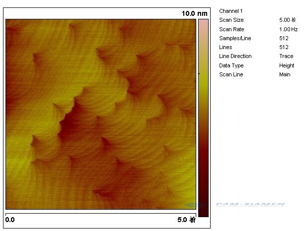
AFM of GaN Epitaxial Template on Sapphire
We also offer custom structure of epitaxial GaN coated sapphire substrates, please see below example:
n-type GaN thin films on c-Al2O3 substrates.
Material: n-type GaN thin film (thickness:1um).
Substrates: c-Al2O3
Size: 2” inch diameter
Electrical resistivity: <0.05 ohm.cm
single side polished.
Source:PAM-XIAMEN

For more information, please contact us email at victorchan@powerwaywafer.com and powerwaymaterial@gmail.com.