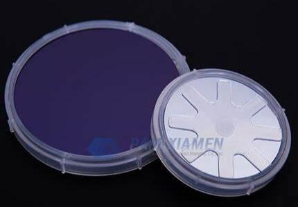
Xiamen Powerway Advanced Material Co., Ltd (PAM-XIAMEN) offers the highest purity InGaAs / InP Epitaxial Wafer in the industry today. Sophisticated manufacturing processes have been put in place to customize and produce high quality InP (Indium Phosphide) Epitaxial wafers up to 4 inches with wavelengths from 1.7 to 2.6μm, ideally suited for high speed, long wavelength imaging, high speed HBT and HEMTs, APDs and analog-digital converter circuits. Applications using InP-based components can greatly exceed transmission rates in comparison to similar components structured on GaAs or SiGe based platforms.

1. InP Epitaxial Wafer Specification
Structure 1: InP epi-wafers EOM (Electro-Optic Modulator) Structure (PAM180828-EOM)
| No | Type of doping | Material | Mole fraction | Thickness, nm | Doping, cm-3 | definition |
| 1 | p++ | In1-xGaxAs | x=0.47
|
– | – | |
| 2 | p+ | InP | – | 1E18 | ||
| 3 | p+ | InP | – | – | ||
| 4 | p | InP | – | – | ||
| 5 | i | InP | 200 | <1E15 | spacer | |
| 6 | MQW | In1-xGaxAsyP1-y/InP | x=0.35
y=0.76 |
12/8
20 periods |
– | WG core |
| 7 | i | InP | – | – | – | spacer |
| 8 | n | InP | – | – | 5E17 | |
| 9 | n+ | InP | – | – | – | |
| 10 | n+ | InP | – | – | – | spacer |
| 11 | i | InP | – | 500 | – | buffer |
| SI InP |
Structure 2:
2″ size InGaAs / InP epitaxial wafer,and we accept custom specs.
Substrate: (100) InP substrate
Epi Layer 1: In0.53Ga0.47As layer , undoped , thickness 200 nm
Epi Layer 2: In0.52Al0.48As layer , undoped , thickness 500 nm
Epi Layer 3:In0.53Ga0.47As layer , undoped , thickness 1000 nm
Top Layer :In0.52Al0.48As layer , undoped , thickness 50 nm
In addition, PAM-XIAMEN can offer the following InP epiwafers:
InGaAs/InP epi wafer for PIN: the InGaAs epitaxial thin film is deposited on the N type or semi-insulating InP (100) wafer doped;
InGaAsP/InGaAs on InP substrates: InP epitaxy wafer is grown with InGaAsP/InGaAs quantum well for fabricating photodiodes;
InGaAs APD Wafers: the epitaxial wafer of InGaAs APD is grown on N type indium phosphide substrate;
InP/InGaAs/InP epi wafer: the epi structure on InP (100) substrate consists of 100nm InGaAs in the first layer (etching stop layer) and 50nm InP in the second layer (bonding layer).
2. About InP based Epi Wafer
Indium Phosphide (InP) is a key semiconductor material that enables optical systems to deliver the performance required for data center, mobile backhaul, metro and long-haul applications. Lasers, photodiodes and waveguides fabricated on InP epitaxial wafers operate at the optimum transmission window of glass fiber, which enable efficient fiber communications. PAM-XIAMEN’s proprietary Etched Facet Technology (EFT) allows wafer level testing similar to traditional semiconductor manufacturing. EFT enables high yield, high performance and reliable lasers. The epi structure grown on GaAs and InP for electronics and optoelectronics is introduced below:
InGaAsP / InP materials prepared on indium phosphide single crystal substrates are used in optical fiber communications, and 1.3~1.6μm light sources and detectors prepared from InGaAs / InP heterojunction materials have been widely used in optoelectronic devices.
In addition, the lattice-matched InGaAs / InP heterojunction can be applied to photodetection in the near-infrared band of 0.9-1.7um. APDs are one of the most important structures in long-distance and high-bit-rate optical fiber communication systems. APD made on GaAs and InP epitaxial structure has the advantages of high response and low dark current. It is widely used in single photon detection and is currently receiving wide attention.
InGaAs / InP epiwafers also can be used to fabricate single-pixel photodiode chips for spectroscopic sensing applications. InGaAs / InP PIN photodiodes have the advantages of simple production, high bandwidth, high sensitivity, and low noise. It is widely used in short-wave infrared detection, so there is an urgent need to prepare high-quality InGaAs / InP epitaxial wafer.
In general, the performance of InGaAs APD or PIN devices strongly depends on the heterogeneous interface of InGaAs / InP and the epitaxial quality of the InGaAs film. At present, solid-state sources (like As2 or As4) are used to grow InP-based InGaAs epitaxial materials. Due to the different adsorption coefficients of As2 and As4, the quality of the grown InGaAs / InP interface is also different. Directly using As2 to grow the InGaAs / InP interface is likely to cause the diffusion of group V atoms.
Therefore, it is necessary to optimize the growth conditions of InGaAs / InP to obtain high crystal quality and interface quality, so as to obtain high-performance optoelectronic properties of the InP wafers.
For more information, please contact us email at victorchan@powerwaywafer.com and powerwaymaterial@gmail.com.

