PAM XIAMEN offers PECVD Nitride
PECVD nitride is an alternative to LPCVD nitride when lower temperature ranges are required. Micro-mechanicalWidely used in Micro-Electro-Mechanical Systems (MEMS) and semiconductor processing, PECVD nitride is a tensile stress film that can be used as a passivation layer or to help balance film stress within a stack. PECVD nitride reduces overall film stress. This prevents delaminating and micro-cracking.
Low Stress PECVD Niride thicker films service is also availble.
PECVD Deposition
Standard Oxide
Slow deposition Oxide
OxyNitride with custom refractive index
Standard Nitride
Low Stress Nitride
About PECVD
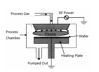
Plasma-enhanced chemical vapor deposition (PECVD) is a method of epitaxy in chemical vapor deposition by exciting gas to generate low-temperature plasma to enhance the chemical activity of reactive species. This method can form solid films at lower temperatures. LPCVD system is shown as figure below:
PECVD Reaction Structure
For example, the matrix material is placed on the cathode in a reaction chamber, the reaction gas is fed to a lower pressure (1-600Pa), and the matrix is kept at a certain temperature. A glow discharge is generated in a certain way, the gas near the surface of the substrate is ionized, and the reactive gas is activated. At the same time, cathode sputtering occurs on the surface of the substrate, thereby improving the surface activity. There are not only the usual thermochemical reactions on the surface, but also complex plasma chemical reactions. The deposited film is formed under the combined action of these two chemical reactions. The methods of exciting glow discharge mainly include: radio frequency excitation, DC high voltage excitation, pulse excitation and microwave excitation.
The main advantages of plasma-enhanced chemical vapor deposition are that the deposition temperature is low, and the impact on the structure and physical properties of the substrate is small; the film thickness and composition uniformity are good; the film structure is dense, with few pinholes.
Films such as silicon dioxide can be deposited by PECVD on metal interconnect layers with lower melting points. In addition, PECVD has a faster deposition rate and better step coverage. It can deposit most mainstream dielectric films, including some advanced low-k materials, hard mask etc.

For more information, please contact us email at victorchan@powerwaywafer.com and powerwaymaterial@gmail.com.