We are an expert of semiconductor wafers in semiconductor industry, and we offer technology support and wafers selling for thousands of univerisities and industrial customers by our decades experience, including Cornell University, Stanford Univeristy,Peking University, Shandong Univerity, university of south carolina,Caltech Faraon lab (USA),University of California, Irvine (USA),Singapore MIT Alliance for Research and Technology Centre (SMART),West Virginia University,Purdue Univerity, University of California, Los Angeles,King Abdullah University of Science & Technology,Massachusetts Institute of Technology,University of Houston,University of Wisconsin,University of Science and Technology of China etc.
And now we show one article example as follows, who bought our wafers or service:
Article title:Characterization and comparison of commercially available silicon carbide (SIC) power switches
Published by:
K. Haehre ; M. Meisser ; F. Denk ; R. Kling
Karlsruhe Instiute of Technology (KIT), Light Technology Institute (LTI), Germany, Engesserstr. 13, D-76131 Karlsruhe
Picture of SiC wafer:

Abstract
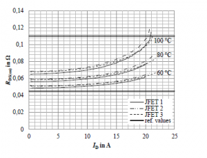
In this paper the electrical and thermal characteristics of commercially available SiC devices, normally-on and -off JFETs as well as a MOSFET, and of a high-voltage Si- MOSFET are presented. The mentioned characteristics are compared and it is shown which characteristics are the limiting factors when designing power electronics devices based on SiC power switches.
Subjuect(s):SiC;JFET;MOSFET;switching-losses;thermal analysis
Article abstract for Using Wafer from Xiamen Powerway Advanced Material Co. Ltd. (PAM-XIAMEN) or Powerway Wafer Co.,Limited
“… [9] J. Lutz, H. Schlangenotto, U. Scheuermann and R. De Doncker, Semiconductor Power Devices,Heidelberg: Springer-Verlag, 2011. [10] XIAMEN POWERWAY ADVANCED MATERIAL CO.,ISilicon Carbide Substrates – Product Specifications,” Xiamen, China, 2011 …”
Source:https://ieeexplore.ieee.org/abstract/document/6242017/authors
About Xiamen Powerway Advanced Material Co., Ltd
PAM-XIAMEN offers semiconductor silicon carbide wafers,6H SiC and 4H SiC wafer in different quality grades for researcher and industry manufacturers. We has developed SiC crystal growth technology and SiC wafer processing technology. We provide custom thin film (silicon carbide)SiC epitaxy on 6H or 4H substrates for the development of silicon carbide devices. SiC epi wafer is mainly used for Schottky diodes, metal-oxide semiconductor field-effect transistors, junction field effect.
PAM-XIAMEN also offer GaAs/InP and GaN material from wafer substrate to epitaxial growth.
Powerway Wafer Co.,Limited is a sub company of Xiamen Powerway Advanced Material Co., Ltd specialize in dealing with overseas orders.
Are You Looking for an Semiconductor wafer?
PAM-XIAMEN is proud to offer semiconductor wafer inlcuidng SiC/GaN/GaAs/InP wafer with wafer or epitaxial wafer for all different kinds of projects. If you are looking for semiconductor wafer, send us enquiry today to learn more about how we can work with you to get you the substrate wafers you need for your next project. Our group team is looking forward to providing both quality products and excellent service for you! For more information, please visit our website:www.powerwaywafer.com, send us email at tech@powerwaywafer.com or powerwaymaterial@gmail.com.