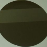


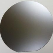

InAs-Wafer
PAM-XIAMEN offers Compound Semiconductor InAs wafer – indium arsenide wafer which are grown by LEC(Liquid Encapsulated Czochralski) as epi-ready or mechanical grade with n type, p type or semi-insulating in different orientation(111) or (100). In addition, InAs single crystal has high electron mobility and is an ideal material for making Hall devices.
- Beschreibung
Produktbeschreibung
PAM-XIAMEN offers Compound Semiconductor InAs wafer – indium arsenide wafer which is grown by LEC(Liquid Encapsulated Czochralski) as epi-ready or mechanical grade with n type, p type or semi-insulating in different orientation(111)(100) or (110). In addition, InAs single crystal has high electron mobility and is an ideal material for making Hall devices.
Indium arsenide, InAs, is a semiconductor composed of indium and arsenic. It has the appearance of grey cubic crystals with a melting point of 942 °C and lattice constant of 0.6058nm, and the indidum arsenide crystal structure is a zinc blende structure. Indium arsenide wafer is used for construction of infrared detectors, for the wavelength range of 1–3.8 µm. The detectors are usually photovoltaic photodiodes. Cryogenically cooled detectors have lower noise, but InAs detectors can be used in higher-power applications at room temperature as well. Because of the superior indium arsenide properties, indium arsenide thin films are also used for making of diode lasers.
Indium arsenide band gap is a direct transition, which is similar to gallium arsenide, and the forbidden band width is (300K)0.45eV. Indium arsenide is sometimes used together with indium phosphide. Alloyed with gallium arsenide, it forms indium gallium arsenide – a material with band gap dependent on In/Ga ratio, a method principally similar to alloying indium nitride with gallium nitride to yield indium gallium nitride.
Hier ist die ausführliche Beschreibung:
2 "(50,8 mm) InAs Wafer-Spezifikation
3 "(76,2 mm) InAs Wafer Specification
4 "(100 mm) Wafer InAs Specification
2 "InAs Wafer-Spezifikation
| Artikel | Technische Daten | |||
| Dotierstoff | low doped | Stannum | Schwefel | Zink |
| Conduction Typ | N-Typ | N-Typ | N-Typ | P-Typ |
| Wafer-Durchmesser | 2 " | |||
| Wafer Orientation | (111)±0.5° , (110)±0.5° | |||
| Waferdicke | 500 ± 25 um | |||
| Primäre Wohnung Länge | 16 ± 2mm | |||
| Secondary Wohnung Länge | 8 ± 1mm | |||
| Ladungsträgerkonzentration | 5×1016cm-3 | (5-20)x1017cm-3 | (1-10)x1017cm-3 | (1-10)x1017cm-3 |
| Mobilität | ≥2×104cm2/V.s | 7000-20000cm2/V.s | 6000-20000cm2/V.s | 100-400cm2/V.s |
| EPD | <5×104cm-2 | <5×104cm-2 | <3×104cm-2 | <3×104cm-2 |
| TTV | <10um | |||
| BOGEN | <10um | |||
| KETTE | <12um | |||
| Laserbeschriftung | auf Anfrage | |||
| suface Finish | P / E, P / P | |||
| Epi bereit | ja | |||
| Paket | Single-Wafer-Behälter oder Kassette | |||
3″ InAs Wafer Specification
| Artikel | Technische Daten | |||
| Dotierstoff | low doped | Stannum | Schwefel | Zink |
| Conduction Typ | N-Typ | N-Typ | N-Typ | P-Typ |
| Wafer-Durchmesser | 3" | |||
| Wafer Orientation | (111)±0.5° , (110)±0.5° | |||
| Waferdicke | 600 ± 25 um | |||
| Primäre Wohnung Länge | 22 ± 2mm | |||
| Secondary Wohnung Länge | 11 ± 1mm | |||
| Ladungsträgerkonzentration | 5×1016cm-3 | (5-20)x1017cm-3 | (1-10)x1017cm-3 | (1-10)x1017cm-3 |
| Mobilität | ≥2×104cm2/V.s | 7000-20000cm2/V.s | 6000-20000cm2/V.s | 100-400cm2/V.s |
| EPD | <5×104cm-2 | <5×104cm-2 | <3×104cm-2 | <3×104cm-2 |
| TTV | <12um | |||
| BOGEN | <12um | |||
| KETTE | <15um | |||
| Laserbeschriftung | auf Anfrage | |||
| suface Finish | P / E, P / P | |||
| Epi bereit | ja | |||
| Paket | Single-Wafer-Behälter oder Kassette | |||
4″ InAs Wafer Specification
| Artikel | Technische Daten | |||
| Dotierstoff | low doped | Stannum | Schwefel | Zink |
| Conduction Typ | N-Typ | N-Typ | N-Typ | P-Typ |
| Wafer-Durchmesser | 4 " | |||
| Wafer Orientation | (111)±0.5° , (110)±0.5° | |||
| Waferdicke | 900 ± 25 um | |||
| Primäre Wohnung Länge | 16 ± 2mm | |||
| Secondary Wohnung Länge | 8 ± 1mm | |||
| Ladungsträgerkonzentration | 5×1016cm-3 | (5-20)x1017cm-3 | (1-10)x1017cm-3 | (1-10)x1017cm-3 |
| Mobilität | ≥2×104cm2/V.s | 7000-20000cm2/V.s | 6000-20000cm2/V.s | 100-400cm2/V.s |
| EPD | <5×104cm-2 | <5×104cm-2 | <3×104cm-2 | <3×104cm-2 |
| TTV | <15um | |||
| BOGEN | <15um | |||
| KETTE | <20um | |||
| Laserbeschriftung | auf Anfrage | |||
| suface Finish | P / E, P / P | |||
| Epi bereit | ja | |||
| Paket | Single-Wafer-Behälter oder Kassette | |||
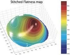
Stitched Flatness Map of InAs Wafer
Wafer Spec(example):
1) 2” (50,8 mm) InAs
Type/Dopant:N/S
Orientation:[111B]±0.5°
Thickness:500±25um
Epi-Ready
SSP
2) 2” (50,8 mm) InAs
Type/Dopant:N/low doped
Orientation : (111)B
Thickness:500um±25um
SSP
3) 2” (50,8 mm) InAs
Type/Dopant:N / low doped
Orientation : <111>A ±0.5°
Thickness:500um±25um
epi-ready
Ra<=0.5nm
Carrier Concentration(cm-3):1E16~3E16
Mobility(cm -2 ):>20000
EPD(cm -2 ):<15000
SSP
4) 2” (50,8 mm) InAs
Type/Dopant:N/low doped
Orientation : <100> with [001]O.F.
Thickness:2mm
AS cut
5) 2” (50,8 mm) InAs
Type/Dopant:N/P
Orientation :(100),
Carrier Concentration(cm-3):(5-10)E17,
Thickness:500 um
SSP
6)Indium Arsenide wafers,
2″Ø×500±25µm,
p-type InAs:Zn
(110)±0.5°,
Nc=(1-3)E18/cc ,
Both-sides-polished,
Sealed under nitrogen in single wafer cassette.
Alle Wafer werden mit hochwertigen Epitaxie bereit Veredelung angeboten. Oberflächen werden durch in-house, fortschrittliche optische Metrologie Techniken charakterisiert, die Surfscan Trübung und Partikelüberwachung, spektroskopische Ellipsometrie und streifendem Einfall Interferometrie umfassen
Der Einfluss der Glühtemperatur auf den optischen Eigenschaften der Oberflächenelektronenanreicherungsschichten in n-Typ (1 0 0) InAs-Wafer wurde durch Raman-Spektroskopie untersucht. Es zeigt, dass Raman-Peaks aufgrund von Streuung durch ungeschirmte LO Phononen mit steigender Temperatur verschwinden, die in der InAs Oberfläche die Elektronenakkumulationsschicht zeigt durch Glühen beseitigt wird. Der beteiligte Mechanismus wurde durch Röntgenstrahl-Photoelektronen-Spektroskopie, Röntgenbeugung und hochauflösende Transmissions-Elektronenmikroskopie analysiert. Die Ergebnisse zeigen, daß amorphes In2O3 und As2O3 Phasen bei InAs Oberfläche während des Glühens und unterdessen gebildet werden, eine dünne kristalline As-Schicht an der Grenzfläche zwischen der oxidierten Schicht und der Wafer wird auch was zu einer Abnahme der Dicke der Oberflächenelektronenakkumulations erzeugten da, wie Schicht Adatome einzuführen Oberflächenzustände Akzeptor-Typ.
The emission wavelength of InAs is 3.34μm, and lattice-matched In-GaAsSb, InAsPSb and InAsSb multi-epitaxial materials can be grown on the indium arsenide substrates, which can manufacture lasers and detectors for optical fiber communication in the 2~4μm band.
We also offer InAs wafer epi service, take below as an example:
2”size InAs epi wafer(PAM190730-INAS):
Epi layer: Thikness 0.5 um, InAs epi layer(undoped, n type),
Substrate:2” semi-insulating GaAs
More details about InAs epi wafer, please refer to:
Relative Produkte:
InAs-Wafer
InSb-Wafer
InP-Wafer
GaAs-Wafer
GaSb-Wafer
GaP-Wafer
Indium Arsenide Ingot with Zinc Blende Structure Grown By VGF
Sie können auch mögen ...
-
GaSb Wafer
PAM-XIAMEN offers Compound Semiconductor GaSb wafer – gallium antimonide which are grown by LEC(Liquid Encapsulated Czochralski) as epi-ready or mechanical grade with n type, p type or semi-insulating in different orientation(111) or (100).
-
GaP-Wafer – kann vorübergehend nicht angeboten werden
PAM-XIAMEN offers Compound Semiconductor GaP wafer – gallium phosphide wafer which is grown by LEC(Liquid Encapsulated Czochralski) as epi-ready or mechanical grade with n type, p type or semi-insulating in different orientation(111)or(100). -
Ge (Germanium) Einkristallen und Oblaten
PAM-XIAMEN bietet 2-Zoll-, 3-Zoll-, 4-Zoll- und 6-Zoll-Germaniumwafer an, die Abkürzung für „Ge-Wafer, gewachsen durch VGF/LEC“. Leicht dotierte Germaniumwafer vom P- und N-Typ können auch für Hall-Effekt-Experimente verwendet werden. Bei Raumtemperatur ist kristallines Germanium spröde und weist eine geringe Plastizität auf. Germanium hat Halbleitereigenschaften. Hochreines Germanium wird mit dreiwertigen Elementen (wie Indium, Gallium, Bor) dotiert, um Germaniumhalbleiter vom P-Typ zu erhalten; und fünfwertige Elemente (wie Antimon, Arsen und Phosphor) werden dotiert, um Germaniumhalbleiter vom N-Typ zu erhalten. Germanium verfügt über gute Halbleitereigenschaften, wie z. B. eine hohe Elektronenmobilität und eine hohe Lochmobilität. -
GaAs Epiwafer
PAM-XIAMEN is manufacturing various types of epi wafer III-V silicon doped n-type semiconductor materials based on Ga, Al, In, As and P grown by MBE or MOCVD. We supply custom GaAs epiwafer structures to meet customer specifications, please contact us for more information.
-
GaN-HEMT-Epitaxie-Wafer
Gallium Nitride (GaN) HEMTs (High Electron Mobility Transistors) are the next generation of RF power transistor technology. Thanks to GaN technology, PAM-XIAMEN now offer AlGaN/GaN HEMT Epi Wafer on sapphire or Silicon, and AlGaN/GaN on sapphire template.
-
SiC-Wafersubstrat
The company has a complete SiC(silicon carbide) wafer substrate production line integrating crystal growth, crystal processing, wafer processing, polishing, cleaning and testing. Nowadays we supply commercial 4H and 6H SiC wafers with semi insulation and conductivity in on-axis or off-axis, available size:5x5mm2,10x10mm2, 2”,3”,4”, 6” and 8″, breaking through key technologies such as defect suppression, seed crystal processing and rapid growth, promoting basic research and development related to silicon carbide epitaxy, devices, etc.
-
InP-Wafer
PAM-XIAMEN offers VGF InP(Indium Phosphide) wafer with prime or test grade including low dope, N type or semi-insulating. The mobility of InP wafer is different in different type, low doped one>=3000cm2/V.s, N type>1000 or 2000cm2V.s(depends on different doping concentration), P type: 60+/-10 or 80+/-10cm2/V.s(depends on different Zn doping concentration), and semi-insulting one>2000cm2/V.s, the EPD of Indium Phosphide is below 500/cm2 normally.
-
InSb-Wafer
PAM-XIAMEN offers Compound Semiconductor InSb wafer – Indium antimonide wafer which is grown by LEC(Liquid Encapsulated Czochralski) as epi-ready or mechanical grade with n type, p type or semi-insulating in different orientation(111) or (100). Indium antimonide doped with isoelectronic(such as N doping) can reduce the defect density during the indium antimonide thin films manufacturing process.