GaN-HEMT-Epitaxie-Wafer
Gallium Nitride (GaN) HEMTs (High Electron Mobility Transistors) are the next generation of RF power transistor technology. Thanks to GaN technology, PAM-XIAMEN now offer AlGaN/GaN HEMT Epi Wafer on sapphire or Silicon, and AlGaN/GaN on sapphire template.
- Beschreibung
Produktbeschreibung
GaN HEMT epitaxial wafer is a multilayer film grown epitaxially on a substrate, which usually includes a nucleation layer, a transition layer, a buffer layer, a channel layer, a barrier layer, a cap layer, and a passivation layer from bottom to top. The nucleation layer, like AlGaN or AlN, is used to prevent the substrate material from diffusing into the GaN epitaxial layer. The transition layer may contain hierarchical AlGaN, AlN/GaN superlattice or multilayer AlN to balance the stress between the GaN and the substrate. The higher the Al content in the barrier layer of AlGaN, the higher the 2DEG concentration at the heterojunction. Meanwhile, the lower the threshold voltage of the device, and the higher the current capacity. As the Al ratio increasing, the degree of heterogeneous crystal lattice mismatch will be higher, resulting in a decrease in gallium nitride HEMT electron mobility and a decrease in current capacity.
The High Electron Mobility Transistor (HEMT) is developed based on GaN with unique heterostructure and two-dimensional electron gas. The GaN HEMT advantages include high breakdown strength, low on-resistance and faster The switching speed, which is very suitable for medium and low voltage and medium and small power systems, such as travel adapters, wireless chargers, AC-DC converters, smart home appliances, etc. The epitaxial wafer with HEMT structure is more attractive currently for high-frequency converters, in which GaN HEMT breakdown voltage is 600~650 V. With the rapid development of gallium nitride HEMT epi technology, the price of GaN HEMT devices will be competitive, which can gain large GaN HEMT market for GaN HEMT manufacturers. Moreover, due to the gallium nitride HEMT reliability, it can be widely used in industrial fields, such as photovoltaic inverters, energy storage systems, and electric vehicles.
1. GaN HEMT Material: Available size:2”,4”,6”,8”:
More specific parameters of gallium nitride HEMT wafer for D-mode GaN HEMTs, E-mode GaN HEMTs, GaN HEMT power amplifier and RF, please refer to:
GaN auf Si für Energie, D-Modus
GaN auf Si für Energie, E-Modus
We are expert in HEMT structure, we also offer GaN HEMT epi wafer for many years.
For silicon substrate, we need to know if you grow GaN HEMT on silicon for POWER or RF, it is different. If needed, please contact victorchan@powerwaywafer.com for details.
For SiC, you should use semi-insulating.
Or you can buy AlGaN/GaN HEMT structure on these three structure from us.
2. Now we show you an example as follows:
2.1 2 "(50,8 mm) GaN HEMT Epitaxiewafern
We offer 2″(50.8mm) gallium nitride HEMT Wafers, the GaN HEMT structure is as follows:
Struktur (von oben nach unten):
* Undotierte GaN Kappe (2 ~ 3 nm)
AlxGa1-xN (18 ~ 40 nm)
AlN (Pufferschicht)
undotiertes GaN (2 ~ 3um)
Saphirsubstrat
* Wir können Si3n verwenden GaN auf der Oberseite zu ersetzen, ist die Haftung stark, es durch Sputter oder PECVD beschichtet ist.
2.2 AlGaN/GaN HEMT Epi Wafer on sapphire/GaN
| Schicht # | Zusammensetzung | Dicke | X | Dotierstoff | Ladungsträgerkonzentration |
| 5 | GaN | 2 nm | – | – | – |
| 4 | AlxGa1–xN | 8 nm | 0.26 | – | – |
| 3 | AlN | 1nm | Undotierte | ||
| 2 | GaN | ≥1000 nm | Undotierte | ||
| 1 | Buffer / Übergangsschicht | – | – | ||
| Substrat | Silizium | 350 um / 625μm | – | ||
2.3 2″(50.8mm),4″ (100mm)AlGaN/GaN HEMT Epi Wafer on Si
2.3.1 Specifications for Aluminium Gallium Nitride (AlGaN) / Gallium Nitride (GaN) HEMT (HEMT) auf einem Siliziumsubstrat.
| Bedarf | Spezifikation |
| AlGaN / GaN HEMT Epi-Wafer auf Si | |
| AlGaN / GaN HEMT-Struktur | siehe 1.2 |
| Substratmaterial | Silizium |
| Orientierung | <111> |
| Wachstumsverfahren | float Zone |
| Conduction Typ | P oder N |
| Größe (Zoll) | 2” , 4” |
| Dicke (um) | 625 |
| Hintern | rau |
| Der spezifische Widerstand (Ω-cm) | >6000 |
| Bogen (um) | ≤ ± 35 |
2.3.2 Epi structure: Crack-free Epilayers
| Schicht # | Zusammensetzung | Dicke | X | Dotierstoff | Ladungsträgerkonzentration |
| 5 | GaN | 2 nm | – | – | – |
| 4 | AlxGa1–xN | 8 nm | 0.26 | – | – |
| 3 | AlN | 1nm | Undotierte | ||
| 2 | GaN | ≥1000 nm | Undotierte | ||
| 1 | Buffer / Übergangsschicht | – | – | ||
| Substrat | Silizium | 350 um / 625μm | – | ||
2.3.3 Electrical Properties of the AlGaN/GaN HEMT structure
2DEG Mobility (bei 300 K): ≥1,800 cm2 / Vs
2DEG Blatt Trägerdichte (bei 300 K): ≥0.9 × 1013 cm-2
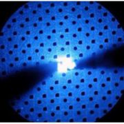
RMS-Rauhigkeit (AFM): ≤ 0,5 nm (5,0 & mgr; m × 5,0 & mgr; m-Scan-Bereich)
2.4 2″(50.8mm)AlGaN/GaN on sapphire
Zur Spezifikation von AlGaN / GaN auf Saphir-Vorlage, bitte an unsere Verkaufsabteilung: sales@powerwaywafer.com.
GaN HEMT Applications: Used in blue laser diodes, ultraviolet LEDs (down to 250 nm), and AlGaN/GaN HEMTs device.
3. Explanation of AlGaN/Al/GaN HEMTs:
Nitride HEMTs werden für Hochleistungselektronik in Hochfrequenz-Verstärkung und Leistungsschaltanwendungen intensiv entwickelt. Oft hohe Leistung in DC-Betrieb verloren, wenn der HEMT schaltet ist - zum Beispiel des auf Strom kollabiert, wenn das Gate-Signal gepulst wird. Es wird vermutet, dass solche Effekte zu Charge-Trapping in Zusammenhang stehen, dass Masken die Wirkung des Tores auf dem Stromfluss. Feldplatten auf den Source- und Gate-Elektroden sind verwendet worden, um das elektrische Feld in der Vorrichtung zu manipulieren, wie Strom-collapse Erscheinungen abzuschwächen.
4. GaN EpitaxialTechnology — Customized GaN epitaxy on SiC,Si and Sapphire substrate for HEMTs, LEDs:
GAN HEMT Epitaxiewafern (GAN EPI-WAFER)
PAM XIAMEN Offers Epitaxial growth of AlGaN/GaN based HEMT on Si wafers
5. GaN Device:
GaN HEMT
6. Test Characterization Equipment:
Berührungslose Flächenwiderstand
Laser Thin Film Dicke Mapping
High Temp / Hochfeuchte- Rückwärts-Bias
Thermoschock
DIC Nomarski-Mikroskop
Atomkraftmikroskop (AFM)
Oberflächen Fehlerhaftigkeit Scan
High Temp Rückwärts-Bias
4PP Flächenwiderstand
Contactless Halle Mobility
Temperaturzyklus
X-ray Diffraction (XRD) / Reflektanz (XRR)
Ellipsometer Dicke
Profilometer
CV Tester
7. Foundry Fabrication:
we also offer foundry GaN HEMT fabrication in the following process as follows:
MOCVD-Epitaxie
Metall-Sputter / E-Beam-
Dry / Wet Metal / Dielektrikumätzen
Thin Film PECVD / LPCVD / Sputtering
RTA / Ofentemperung
Fotolithografie (0,35 um min. CD)
Ionenimplantation
Remark:
The Chinese government has announced new limits on the exportation of Gallium materials (such as GaAs, GaN, Ga2O3, GaP, InGaAs, and GaSb) and Germanium materials used to make semiconductor chips. Starting from August 1, 2023, exporting these materials is only allowed if we obtains a license from the Chinese Ministry of Commerce. Hope for your understanding and cooperation!
More fabrication services, please visit: GaN Fabrication Services for HEMT Devices
Aluminium gallium arsenide epi wafer
650V GaN FETs Chip for Fast Charge
GaN MOSFET Structure:
GaN MOSFET Structure on SiC Substrate
More about GaN HEMT structures, please read:
Sie können auch mögen ...
-
GaN-basierte LED-Epitaxialwafer
PAM-Xiamens GaN (Galliumnitrid) -basierte LED-Epitaxialwafer ist für ultra hohe Helligkeit blaue und grüne lichtemittierenden Dioden (LED) und Laserdioden (LD) Anwendung.
-
GaN-Vorlagen
PAM-Xiamens Template-Produkte bestehen aus kristallinen Schichten (Galliumnitrid) GaN-Vorlagen (Aluminiumnitrid) AlN schablonen (Aluminium-Gallium-Nitrid) AlGaN Vorlagen und (Indium-Gallium-Nitrid) InGaN-Vorlagen, die auf Saphir abgeschieden werden, -
GaAs Epiwafer
PAM-XIAMEN is manufacturing various types of epi wafer III-V silicon doped n-type semiconductor materials based on Ga, Al, In, As and P grown by MBE or MOCVD. We supply custom GaAs epiwafer structures to meet customer specifications, please contact us for more information.
-
SiC-Wafersubstrat
The company has a complete SiC(silicon carbide) wafer substrate production line integrating crystal growth, crystal processing, wafer processing, polishing, cleaning and testing. Nowadays we supply commercial 4H and 6H SiC wafers with semi insulation and conductivity in on-axis or off-axis, available size:5x5mm2,10x10mm2, 2”,3”,4”, 6” and 8″, breaking through key technologies such as defect suppression, seed crystal processing and rapid growth, promoting basic research and development related to silicon carbide epitaxy, devices, etc.
-
Freistehenden GaN-Substrat
PAM-XIAMEN haben die Fertigungstechnik für freistehende (Galliumnitrid) GaN-Substrat-Wafer festgelegt, die für UHB-LED und LD ist. Grown durch Hydrid-Gasphasenepitaxie (HVPE) Technologie hat sich unser GaN-Substrat mit niedriger Fehlerdichte.
-
Ge (Germanium) Einkristallen und Oblaten
PAM-XIAMEN bietet 2-Zoll-, 3-Zoll-, 4-Zoll- und 6-Zoll-Germaniumwafer an, die Abkürzung für „Ge-Wafer, gewachsen durch VGF/LEC“. Leicht dotierte Germaniumwafer vom P- und N-Typ können auch für Hall-Effekt-Experimente verwendet werden. Bei Raumtemperatur ist kristallines Germanium spröde und weist eine geringe Plastizität auf. Germanium hat Halbleitereigenschaften. Hochreines Germanium wird mit dreiwertigen Elementen (wie Indium, Gallium, Bor) dotiert, um Germaniumhalbleiter vom P-Typ zu erhalten; und fünfwertige Elemente (wie Antimon, Arsen und Phosphor) werden dotiert, um Germaniumhalbleiter vom N-Typ zu erhalten. Germanium verfügt über gute Halbleitereigenschaften, wie z. B. eine hohe Elektronenmobilität und eine hohe Lochmobilität. -
GaSb Wafer
PAM-XIAMEN offers Compound Semiconductor GaSb wafer – gallium antimonide which are grown by LEC(Liquid Encapsulated Czochralski) as epi-ready or mechanical grade with n type, p type or semi-insulating in different orientation(111) or (100).
-
Float-Zone monokristallinem Silizium
PAM-XIAMEN kann Float-Zone-Siliziumwafer anbieten, die nach dem Float-Zone-Verfahren hergestellt werden. Monokristalline Siliziumstäbe werden durch Wachstum in der Floatzone gewonnen und anschließend werden die monokristallinen Siliziumstäbe zu Siliziumwafern verarbeitet, die als Floatzonen-Siliziumwafer bezeichnet werden. Da der zonengeschmolzene Siliziumwafer während des Schwebezonen-Siliziumprozesses keinen Kontakt mit dem Quarztiegel hat, befindet sich das Siliziummaterial in einem suspendierten Zustand. Dadurch wird es während des Schwebezonenschmelzprozesses von Silizium weniger verschmutzt. Der Kohlenstoffgehalt und der Sauerstoffgehalt sind geringer, die Verunreinigungen sind geringer und der spezifische Widerstand ist höher. Es eignet sich für die Herstellung von Leistungsgeräten und bestimmten elektronischen Hochspannungsgeräten.


