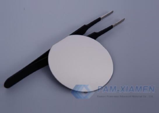
PAM-XIAMEN have round, saw cut, lap and polish gallium antimonide wafers with an epi-ready surface quality for sale. Gallium antimonide crystal is a compound formed by 6N pure Ga and Sb element and is grown by Liquid Encapsulated Czochralski ( LEC ) method with EPD < 1000 cm -3 . GaSb crystal has high uniformity of electrical parameters and low defect density , suitable for MBE or MOCVD epitaxial growth. We have “epi ready ” GaSb semiconductors with wide choice in exact or off orientation , low or high doped concentration and good surface finish.
1. Gallium Antimonide Wafer Substrate Specifications
No.1 PAM-190307-GASB
| Technical Specification | |
| Type | N |
| Dopant | Hi-Te |
| Diameter | 50.8 ± 0.50 mm |
| Orientation | (100)± 0.1° |
| Bow | <10μm |
| Warp | <10μm |
| Mobility | >2500 cm² /V•s |
| Etch Pit Density | <500 cm-2 |
| FWHM | <10 arcsec |
| Thickness | 500 ± 25 um |
| Roughness | RMS <0.5nm |
| Surface Polish | Dual Polish |
No.2 GaSb Wafer 2” or 3”
Orientation:(100)±0.5°
Thickness(μm):500±25;600±25
Type/Dopant:P/undoped;P/Si;P/Zn
Nc(cm-3):(1~2)E17
Mobility(cm2/V ·s):600~700
Growth Method:CZ
Polish:SSP
No.3 2 inch GaSb wafer
Orientation:(100)±0.5°
Thickness(μm):500±25;600±25
Type/Dopant:N/undoped;P/Te
Nc(cm-3):(1~5)E17
Mobility(cm2/V ·s):2500~3500
Growth Method:LEC
Polish:SSP
No.4 2″ GaSb wafer
Orientation:(111)A±0.5°
Thickness(μm):500±25
Type/Dopant:N/Te;P/Zn
Nc(cm-3):(1~5)E17
Mobility(cm2/V ·s):2500~3500;200~500
Growth Method:LEC
Polish:SSP
No.5 50.8mm GaSb Substrate
Orientation:(111)B±0.5°
Thickness(μm):500±25;450±25
Type/Dopant:N/Te;P/Zn
Nc(cm-3):(1~5)E17
Mobility(cm2/V ·s):2500~3500;200~500
Growth Method:LEC
Polish:SSP
No.6 Gallium Antimonide Substrate 50.8mm
Orientation:(111)B 2deg.off
Thickness(μm):500±25
Type/Dopant:N/Te;P/Zn
Nc(cm-3):(1~5)E17
Mobility(cm2/V ·s):2500~3500;200~500
Growth Method:LEC
Polish:SSP
2. Gallium Antimonide Properties
Gallium Antimonite is a III-V compound semiconductor, which belongs to zinc blende, a direct band gap material. The gallium antimonide band gap is 0.725eV at 300K with a lattice constant of 0.60959nm.
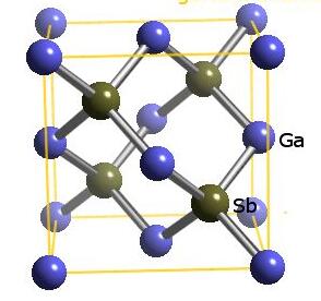
Gallium Antimonide Structure
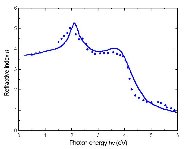
In addition, the gallium antimonide atomic number is 3.53 x 10²² / cm3. On the [100] plane, Ga atoms and Sb atoms are distributed in steps; on the plane, there are the same number of Ga atoms and Sb atoms, but they are easy to cleavage. The [111] plane of GaSb crystals may be composed entirely of Ga atoms, or composed entirely of Sb atoms. Therefore, these two planes have completely different physical and chemical properties. The diagram below shows the changes of gallium antimonide refractive index n with the photon energy at 300 K:
3. LEC Method Growing for GaSb Single Crystal Wafer
Usually the most common method of growing single crystals from the melt is the Czochralski method (CZ). However, for GaSb materials, the Sb element is easier to dissociate and volatilize during the single crystal growth process, which will lead to an imbalance of the Ga:Sb stoichiometric ratio in the melt, resulting in dislocation defects and even distortion into polycrystalline. Therefore, in the process of gallium antimonide single crystal growth, the method of covering the surface of the melt in the ordinary Czochralski crucible with a layer of liquid covering agent is often used to seal the GaSb melt and control the dissociation and volatilization of the Sb element in the melt to achieve the stable growth of GaSb crystals. Such a method is the liquid-sealed Czochralski method (LEC).
However, there are many problems in the process of preparing GaSb crystal wafer by the LEC method. For example, the space in the single crystal furnace is relatively open, and the heat convection in the furnace is relatively complicated. Moreover, the defects of gallium antimonide solid are greatly affected by the drawing process, and the Sb element in polycrystalline material is more volatile.
4. Applications of Gallium Antimonide Crystal Substrate
The band gap of GaSb covers a wide spectral range (0.8~4.3μm), which matches the lattice constants of a variety of ternary and quaternary III-V group compound solid solutions (like InGaAsSb and AlGaSb). Using GaSb as the substrate material to epitaxially grow the above solid solution material can effectively reduce the stress, defects and other problems caused by lattice mismatch.
Because of the excellent physical and chemical properties of GaSb semiconductor, it is often used as a substrate material for infrared detectors and lasers of 8-14mm and larger than 14mm. In addition, Te-doped gallium antimonide substrate can be used to prepare thermal photovoltaic devices and microwave devices with high photoelectric conversion efficiency.
The splitting of its valence band spin orbit can obtain an energy level with an increased hole ionization coefficient, which can improve the signal-to-noise ratio of a long-wavelength avalanche photodetector (APD). Because the critical yield stress of GaSb single crystal is relatively large (15.8N/mm2), its dislocation density is not high (not exceeding 103 orders of magnitude). So it is suitable for making GaInSb/GaAlAsSb lasers, GaInAsSb detectors and GaAs/GaSb laminated solar cells (conversion efficiency exceeds 30%).
Take the gallium antimonide solar cells for example. Compared with ordinary solar cells, thermal photovoltaic cells have the advantage of getting rid of the dependence of ordinary photovoltaic cells on sunlight and using infrared light emitted by fossil fuels, isotopes and nuclear energy to perform photovoltaic effects. The unit power generation of thermal photovoltaic cells is smaller, lighter, and more feasible.
5. FAQ about Gallium Antimonide Substrate
Q1: I have a technical question that how you measure the EPD on the GaSb substrates ?
A: Take samples from the head and tail of the ingot and measure one piece each. After the polished GaSb wafer is corroded, the number of dislocation pits per unit area is statistically calculated by microscope observation.
Q2: In our experience the counting for EPD of GaSb wafer very much depends on the etchant used and on the etching procedure. What do you use?
A: It is a standard dislocation corrosion acid with reliable test results of GaSb EPD measurement. Just control the temperature (room temperature) and corrosion time.

For more information, please contact us email at victorchan@powerwaywafer.com and powerwaymaterial@gmail.com.