Silicon carbide has a variety of crystal types, but the silicon crystal structure the market needed is mainly 4H-SiC. So the silicon carbide crystal growth in crystal types is a defect. To a certain extent, it can be distinguished by the naked eye. A more accurate measurement method for testing the silicon carbide crystal distribution is Raman spectroscopy: Raman spectroscopy has characteristics for crystals, and the peak positions of the light emitted by different crystals are different.
1. What is Raman Spectroscopy?
1928 entdeckte der indische Wissenschaftler Raman die Raman-Streuung im Experiment zur Untersuchung des Streuspektrums von flüssigem Benzol. Raman-Streuspektroskopie bedeutet in einfachen Worten, dass ein auf eine Substanz einfallender Lichtstrahl verwendet wird, die Frequenz des einfallenden Lichts v ist und die Frequenz des resultierenden gestreuten Lichts v, v + Δv1, v-Δv1, v ist + Δv2, v-Δv2 und so weiter. Diese Δv1, Δv2 usw. Δv weisen Eigenschaften auf. Mit anderen Worten, jede Substanz weist einen bestimmten Unterschied (Spitzenposition, Spitzenintensität) auf, der als Raman-Verschiebung (emittiertes Licht minus einfallendes Licht) bezeichnet wird.
Zum Beispiel ist das Raman-Spektrum von 4H-SiC:
| Raman-Verschiebung (cm-1) | E2 transversale Schallwelle | E2 transversale Schallwelle | A1 transversale Schallwelle | E2 transversale Schallwelle | A1 transversale Schallwelle | A1 longitudinale Schallwelle | LOPC | LOPC |
| 4H-SiC | 194.958 | 204.034 | 610.031 | 776.489 | 796.861 | 963.106 | 964.769 | 994.643 |
The table above shown here is the Raman shift. During the silicon carbide crystal distribution measurement, the computer will help to calculate it and process it as a Raman shift spectrum.
2. How to Test the Silicon Carbide Crystal Distrubution?
Typische Testbedingungen sind: Unter Verwendung des 532-nm-Lasers des Ar + -Lasers des LabRAM HR-Raman-Spektrometers fällt er vertikal ein, die Anregungsleistung beträgt 200 mW und der Modus zum Sammeln von Streulicht ist der Rückstreumodus. Das einfallende Licht mit unterschiedlichen Wellenlängen hat unterschiedliche Eindringtiefen. Im Allgemeinen beträgt der 266-nm-Laser 0,2 um, der 325-nm-Laser 2 um und der 514-nm-Laser 30 um, was bedeutet, dass ultraviolettes Licht nur zur Messung dünner Proben verwendet werden kann.
Because the silicon carbide wafer has different positions, multiple measurements will be taken to obtain the silicon carbide crystal distribution:
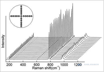
The data has three indicators: the position of the peak, the height of the peak (light intensity), and the width of the peak. Only when the peak position is completely matched, can it be das qualifizierte 4H-SiC. Wie bei der XRD handelt es sich bei allen anderen Peaks um Substanzen anderer Phasen, was ein Defekt ist.
The difference in the position of the peak is due to the difference in the energy of the phonons brought about by the different silicon carbide crystal lattices, that is, the different frequencies. Each phonon has its corresponding energy level. The virtual energy level theory can be used to explain Raman (non-linear process):
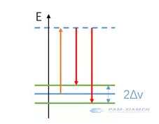
Das Teilchen absorbiert einfallendes Licht auf das virtuelle Energieniveau (orange) und geht dann auf ein Schwingungsenergieniveau (rot) zurück, das sich vom ursprünglichen Energieniveau unterscheidet. Da das obere Energieniveau ein virtuelles Energieniveau ist, kann die Frequenz des einfallenden Lichts variiert werden, solange es nicht mit dem ursprünglichen realen Energieniveau in Konflikt steht.
Es ist erwähnenswert, dass der LOPC-Modus (964,769 cm & supmin; ¹) zur Analyse der Trägerkonzentration verwendet werden kann:
n = 1.25 * 1017cm-2 *(964.769cm-1-VLOPC measurement)
As the carrier concentration increases, the interaction between atoms and the lattice increases, which makes the Raman peak blue shift (smaller), the intensity decreases, and the width increases. This method is not as accurate as other methods and can only be used as an aid to analyze the silicon carbide crystal distribution.
3. Why not Use XRD to Measure Silicon Carbide Crystal Distribution?
X-rays are optical radiation generated by the transition of electrons in the inner layer of atoms under the bombardment of high-speed moving electrons, including continuous X-rays and characteristic X-rays. Silicon carbide single crystal can be used as X-ray gratings, and the coherent scattering produced by these large numbers of particles (atoms, ions, or molecules) will cause light interference, increasing or decreasing the intensity of scattered X-rays. Due to the superposition of scattered waves from a large number of particles, the beams that interfere with each other to produce the highest intensity are called X-ray diffraction lines.
Um die Beugungsbedingungen zu erfüllen, kann die Bragg-Formel angewendet werden: 2dsinθ = nλ.
Der einfallende Strahl bewirkt, dass jeder Streuer einen kleinen Teil seiner Intensität als sphärische Welle zurückstrahlt. Wenn die Streuer symmetrisch zum Intervall d angeordnet sind, werden diese sphärischen Wellen nur in der Richtung synchronisiert, in der ihre Weglängendifferenz 2dsinθ gleich einem ganzzahligen Vielfachen der Wellenlänge λ ist. In diesem Fall wird ein Teil des einfallenden Strahls um einen Winkel von 2 & thgr; abgelenkt, wodurch Reflexionspunkte im Beugungsmuster erzeugt werden.
Use X-rays of known wavelengths to measure the θ angle to calculate the interplanar spacing d, which is used for X-ray structure analysis; the other is to use a silicon carbide seed crystal with a known d to measure the θ angle to calculate the characteristic X-ray wavelength, and then the elements contained in the sample can be found in the existing data.
The measurement formula is 2dSinθ=λ. While the d value among the cubic silicon carbide crystal is close, and the characteristic is not obvious enough, the accurate silicon carbide crystal distribution cannot be precisely determined. For these reasons, it is not suitable to use the XRD to measure the distribution of silicon carbide crystals.

Für weitere Informationen kontaktieren Sie uns bitte per E-Mail unter victorchan@powerwaywafer.com und powerwaymaterial@gmail.com.