PAM-XIAMEN offers PSS patterned sapphire substrate for high brightness GaN based LED EPI growing application. The patterned sapphire substrate wafer ist es, eine trockene Ätzmaske auf dem Saphirsubstrat zu züchten. Die Maske wird durch ein Standardphotolithographieverfahren graviert. Dann wird der Saphir durch ICP-Ätztechnologie geätzt und währenddessen wird die Maske entfernt. Danach wird das GaN-Material auf dem Saphir gezüchtet, so dass die vertikale Epitaxie des GaN-Materials zur horizontalen Epitaxie wird. Die Details des gemusterten Saphirsubstrats sind unten aufgeführt:
PSS-Saphirsubstrat
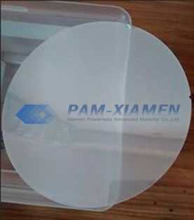
1.SSpezifikations Gemustertes Saphirsubstrat
| Parameter | Spezifikation | Einheit |
| Material | Hochreines monokristallines Al2O3 | |
| Durchmesser | 50,8 ± 0,1 | ㎜ |
| Dicke | 430 ± 10 | ㎛ |
| Variation der Gesamtdicke | ≤10 | ㎛ |
| Primäre flache Länge | 16,0 ± 1,0 | ㎜ |
| Primäre flache Ausrichtung | Eine Ebene ± 0,2 | |
| Qualität der Vorderseite | Epitaxial bereit | |
| Rauheit der Rückseite | 1,0 ± 0,1 | ㎛ |
| Oberflächenorientierung A. | 0˚off ± 0,1 | |
| Oberflächenorientierung M. | 0,2˚off ± 0,10 | |
| Oberflächenorientierung R. | R9 | |
| BOGEN | -10 ~ 0 | ㎛ |
| KETTE | ≤15 | ㎛ |
| Musterbreite | 2,7 ± 0,15 | ㎛ |
| Musterhöhe | 1,7 ± 0,15 | ㎛ |
| Musterabstand | 3,0 ± 0,05 | ㎛ |
2.Warum sollten Sie ein gemustertes Saphirsubstrat für LED wählen?
On the one hand, the cone-shaped patterned sapphire substrate wafer can effectively reduce the dislocation density of the GaN epitaxial material(the patterned sapphire substrate dislocation is low), thereby reducing the non-radiative recombination of the active area, reducing the reverse leakage current, and improving the life of the LED. On the other hand, the light emitted from the active region is scattered multiple times by the interface of GaN and sapphire substrate, and the exit angle of total reflection light is changed, increasing the probability that the light of the flip-chip LED emerges from the sapphire substrate, thereby improving the extraction efficiency of the light.
Zusammenfassend ist die Helligkeit des emittierten Lichts der LED, die auf dem Saphirsubstrat mit Nanomuster gewachsen ist, stark verbessert als die der herkömmlichen LED. Der umgekehrte Leckstrom wird reduziert, was die Lebensdauer der LED verlängert.
A patterned sapphire substrate belongs to the semiconductor industry. As a high-brightness epitaxial material, it is the source material of the LED lighting industry. Meanwhile, using PSS Al2O3 wafer to grow epitaxial wafers is the most effective way to improve the brightness of the chip. It is also the best choice for the high-power and high-brightness epitaxial wafers.

Für weitere Informationen kontaktieren Sie uns bitte per E-Mail unter victorchan@powerwaywafer.com und powerwaymaterial@gmail.com.