Dia 3 inch semi insulating GaAs substrate is available. GaAs materials are mainly divided into two categories: semi-insulating gallium arsenide material and semiconductor gallium arsenide material. Here we will discuss the semi-insulating gallium arsenide material. Semi-insulating property is a basic physical property of gallium arsenide material, and it is a very important property. Through regional ion implantation, the inside of the semi-insulating gallium arsenide substrate an still maintain electrical isolation. So the semi-insulating GaAs substrate is very suitable for the production of integrated circuits. In addition, the parasitic capacitance of the device made of semi-insulating gallium arsenide substrate is very small, which can be used to manufacture some fast devices, such as monolithic microwave integrated circuits. please see below specification:
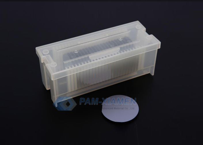
1. Specification of Semi Insulating GaAs Substrate 3 Inch
| Parameter | Technische Daten |
| Material | VGF GaAs-Einkristall-Wafer |
| Klasse | Prime, Epi-Ready |
| Doping | Semi-Insulating, C doped |
| Wafer OD | 76,2 +/- 0,63 mm |
| Wafer Orientation | (100) +/- 0,25 Grad. |
| Primäre Wohnung Länge | 22,22 +/- 3,17 mm |
| Secondary Wohnung Länge | 11,15 +/- 1,52 mm |
| Primäre Wohnung Standort | (01-1) +/- 0.5◦ deg. (US SEMI) |
| sekundäre Wohnung Location |
(011) +/- 0,5 Grad. (US SEMI) |
| Primary / Secondary Wohnung Orientation |
90◦ +/- 0.5◦ |
| Secondary Wohnung ist senkrecht zur Primär Wohnung in Richtung gegen den Uhrzeigersinn | |
| Ladungsträgerkonzentration | <1E8 / cc |
| Der spezifische Widerstand | > 1E7Ohm-cm |
| Mobilität | > 6000 cm 2 / V-sec |
| EPD | <5000 / cm2 |
| Dicke | 625 +/- 25 um |
| TTV | </ = 8.00μm |
| Bogen | </ = 10.00μm |
| Oberflächenfinish | Seite 1: Poliert Side 2 : Etched |
| Laser-Markierung | Auf der Vorderseite, in der Nähe von Haupt Wohnung (Vendor to provide Wafer identification Number on the Wafer near the Major Flat) |
| Qualität | Kratzer, Edge-Chips, Sawmarks, Cracks, Pits, Haze & Orange peel should not be present. |
| HALB Norm | M 9,2-89 |
2. Application and Significance of Semi-insulating GaAs Substrate
Gallium arsenide materials are mainly divided into two categories: semi-insulating gallium arsenide materials and semiconductor gallium arsenide materials. Semi insulating gallium arsenide materials are mainly used to produce integrated circuits with MESFET, HEMT and HBT structures, and mainly used in radar, microwave and millimeter wave communications, ultra-high-speed computers and optical fiber communications.
In the field of microelectronics, semi-insulating GaAs is used as the substrate. Due to the characteristics of high electron mobility, large band gap, direct band gap, and low power consumption, semi-insulating substrates are used to make high-speed digital circuits, microwave monolithic circuits, optoelectronics, and integrated circuits and high-power field effect transistors, which have the characteristics of fast speed, high frequency, low power consumption and radiation resistance. Semi insulating substrate is not only of great significance in national defense, but also widely used in civil and national economic construction. In the communication field, semi-insulating gallium arsenide materials are mainly used in high-frequency communication devices. In recent years, driven by the civilian wireless communication market, especially the mobile phone market, the semi insulating GaAs substrate market scale has also grown rapidly. In the process of commercialization of 5G, it plays an irreplaceable role.

Für weitere Informationen kontaktieren Sie uns bitte per E-Mail untervictorchan@powerwaywafer.com und powerwaymaterial@gmail.com.