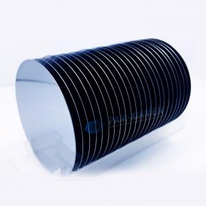
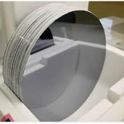
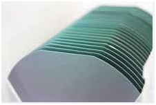
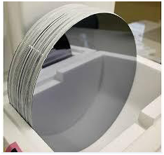
Epitaxialer Siliziumwafer
Silicon Epitaxial Wafer(Epi Wafer) is a layer of epitaxial silicon single crystal deposited onto a single crystal silicon wafer(note: it is available to grow a layer of poly crystalline Silicon layer on top of a highly doped Singly crystalline silicon wafer, but it needs buffer layer (such as oxide or poly-Si) in between the bulk Si substrate and the top epitaxial silicon layer. It also can be used for thin film transistor.
- Beschreibung
Produktbeschreibung
Siliziumepitaxialwafers
Silicon Epitaxial Wafer(Epi Wafer)is a layer of epitaxial silicon single crystal deposited onto a single crystalSiliziumwafer(note: it is available to grow a layer of poly crystalline Silicon layer on top of a highly doped Singly crystalline silicon wafer, but it needs buffer layer (such as oxide or poly-Si) in between the bulk Si substrate and the top epitaxial silicon layer. It also can be used for thin film transistor.
The methods for preparing epitaxial silicon wafers include vapor phase epitaxy, liquid phase epitaxy, molecular beam epitaxy and so on. Among them, chemical vapor deposition (CVD)-based vapor phase epitaxy is the main silicon epitaxial growth process. Commonly used sources are SiCl4, SiHCl3, SiH2Cl2 and SiH4.
In order to meet the needs of various semiconductor devices, various silicon epitaxial technologies have been generated for epitaxial silicon wafer production. In addition to the silicon epitaxial growth in low temperature epitaxy and reduced pressure epitaxy, there is also selective epitaxy that deposits a silicon epitaxial layer on a specific part of the silicon wafer.
Die Epitaxieschicht kann beim Abscheiden auf die genaue Dotierungskonzentration dotiert werden, während die Kristallstruktur des Substrats fortgesetzt wird.
Epilayer-Widerstand: <1 Ohm-cm bis 150 Ohm-cm
Epilayer-Dicke: <1 um bis zu 150 um
Struktur: N / N +, N- / N / N +, N / P / N +, N / N + / P-, N / P / P +, P / P +, P- / P / P +.
Wafer-Anwendung: Digital-, Linear-, Power-, MOS- und BiCMOS-Geräte.
Unsere Vorteile auf einen Blick
1.Advanced epitaxial growth equipment, test equipment and epitaxial silicon technology.
2. Bieten Sie höchste Qualität bei geringer Fehlerdichte und guter Oberflächenrauheit.
3.Starker Support des Forschungsteams und technologischer Support für unsere Kunden
150 mm Wafer-Spezifikation:
| Artikel | Spezifikation | |
| Substrat | Subspezifikation Nr. | |
| Barrenwachstumsmethode | CZ | |
| Leitfähigkeitstyp | N | |
| Dotierstoff | Als | |
| Orientierung | (100) ± 0,5 ° | |
| Der spezifische Widerstand | ≤ 0,005 Ohm cm | |
| RRG | ≤15% | |
| [Oi] Inhalt | 8 ~ 18 ppma | |
| Durchmesser | 150 ± 0,2 mm | |
| Primäre Wohnung Länge | 55 ~ 60 mm | |
| Primäre Wohnung Standort | {110} ± 1 ° | |
| Zweitens flache Länge | halb | |
| Zweitens flache Lage | halb | |
| Dicke | 625 ± 15 um | |
| Rückseite Eigenschaften: | ||
| 1 、 BSD / Poly-Si (A) | 1.BSD | |
| 2 、 SIO2 | 2.LTO: 5000 ± 500 A. | |
| 3 、 Kantenausschluss | 3.EE:?0.6 mm | |
| Laserbeschriftung | KEINER | |
| Vorderseite | Spiegel poliert | |
| Epi | Struktur | N / N + |
| Dotierstoff | Phos | |
| Dicke | 3 ± 0,2 um | |
| Thk.Uniformity | ≤5% | |
| Messposition | Mitte (1 Punkt) 10 mm von der Kante entfernt (4 Punkte bei 90 Grad) | |
| Berechnung | [Tmax-Tmin] ÷ [[Tmax + Tmin] X 100% | |
| Der spezifische Widerstand | 2,5 ± 0,2 Ohm cm | |
| Res.Uniformity | ≤5% | |
| Messposition | Mitte (1 Punkt) 10 mm von der Kante entfernt (4 Punkte bei 90 Grad) | |
| Berechnung | [Rmax-Rmin] ÷ [[Rmax + Rmin] X 100% | |
| Stapelfehlerdichte | ≤2 (ea / cm2) | |
| Dunst | KEINER | |
| Scratches | KEINER | |
| Krater 、 Orangenschale 、 | KEINER | |
| Randkrone | ≤ 1/3 Epi-Dicke | |
| Schlupf (mm) | Gesamtlänge ≤ 1Dia | |
| Fremdstoff | KEINER | |
| Kontamination der Rückseite | KEINER | |
| Gesamtpunktfehler (Partikel) | ≤ 30 @ 0,3 um |
Silicon Epitaxy Growth with Boron Dopant by VPE
Epitaxy Wafer of Silicon for Integrated Waveguide Optics
Sie können auch mögen ...
-
GaAs Epiwafer
PAM-XIAMEN is manufacturing various types of epi wafer III-V silicon doped n-type semiconductor materials based on Ga, Al, In, As and P grown by MBE or MOCVD. We supply custom GaAs epiwafer structures to meet customer specifications, please contact us for more information.
-
Float-Zone monokristallinem Silizium
PAM-XIAMEN kann Float-Zone-Siliziumwafer anbieten, die nach dem Float-Zone-Verfahren hergestellt werden. Monokristalline Siliziumstäbe werden durch Wachstum in der Floatzone gewonnen und anschließend werden die monokristallinen Siliziumstäbe zu Siliziumwafern verarbeitet, die als Floatzonen-Siliziumwafer bezeichnet werden. Da der zonengeschmolzene Siliziumwafer während des Schwebezonen-Siliziumprozesses keinen Kontakt mit dem Quarztiegel hat, befindet sich das Siliziummaterial in einem suspendierten Zustand. Dadurch wird es während des Schwebezonenschmelzprozesses von Silizium weniger verschmutzt. Der Kohlenstoffgehalt und der Sauerstoffgehalt sind geringer, die Verunreinigungen sind geringer und der spezifische Widerstand ist höher. Es eignet sich für die Herstellung von Leistungsgeräten und bestimmten elektronischen Hochspannungsgeräten.
-
GaN-Vorlagen
Die Template-Produkte von PAM-XIAMEN bestehen aus kristallinen Schichten von (Galliumnitrid) GaN-Templates, (Aluminiumnitrid) AlN-Template, (Aluminiumgalliumnitrid) AlGaN-Templates und (Indiumgalliumnitrid) InGaN-Templates, die auf Saphir abgeschieden werden -
SiC-Epitaxie
Wir bieten kundenspezifische SiC-Epitaxie für Dünnschichten (Siliciumcarbid) auf 6H- oder 4H-Substraten für die Entwicklung von Siliciumcarbid-Bauelementen an. SiC-Epi-Wafer wird hauptsächlich für Schottky-Dioden, Metalloxid-Halbleiter-Feldeffekttransistoren und Sperrschicht-Feldeffekt verwendet -
Cz monokristallinem Silizium
PAM-XIAMEN, a monocrystalline bulk silicon producer, can offer <100>, <110> and <111> monocrystalline silicon wafers with N&P dopant in 76.2~200 mm, which are grown by CZ method. The Czochralski method is a crystal growth method, referred to as the CZ method. It is integrated in a straight-tube heat system, heated by graphite resistance, melts the polysilicon contained in a high-purity quartz crucible, and then inserts the seed crystal into the surface of the melt for welding. After that, the rotating seed crystal is lowered and melted. The body is infiltrated and touched, gradually raised, and finished or pulled through the steps of necking, necking, shouldering, equal diameter control, and finishing.
-
polierte Wafer
PAM-XIAMEN can offer polished wafer, n type or p type with orientation at <100>, <110> or <111>. FZ polished wafers, mainly for the production of silicon rectifier (SR), silicon controlled rectifier (SCR), Giant Transistor (GTR), thyristor (GRO)
-
Ätzen Wafer
The etching silicon wafers offered by PAM-XIAMEN are N type or P type etching wafers, which have low roughness, low reflectivity and high reflectivity. The etching wafer has the characteristics of low roughness, good glossiness and relatively low cost, and directly substitutes the polished wafer or epitaxial wafer which has relatively high cost to produce the electronic elements in some fields, reducing the costs.
-
Test-Wafer-Monitor Wafer Dummy-Wafer
Als Dummy-Wafer-Hersteller bietet PAM-XIAMEN Silikon-Dummy-Wafer/Test-Wafer/Monitor-Wafer an, die in einem Produktionsgerät verwendet werden, um die Sicherheit zu Beginn des Produktionsprozesses zu verbessern und zur Lieferkontrolle und Bewertung der Prozessform verwendet werden. Da für Experimente und Tests häufig Dummy-Siliziumwafer verwendet werden, sind Größe und Dicke in den meisten Fällen wichtige Faktoren. Es sind 100 mm, 150 mm, 200 mm oder 300 mm Dummy-Wafer erhältlich.


Ähnliche Produkte
-
12 "Prime Grade Silicon Wafer
PAM-XIAMEN bietet blanke 300-mm-Siliziumwafer (12 Zoll) in erstklassiger Qualität, n-Typ oder p-Typ, und die 300-mm-Siliziumwaferdicke beträgt 775 ± 15. Im Vergleich zu anderen Siliziumwafer-Anbietern ist der Preis für Siliziumwafer von Powerway Wafer wettbewerbsfähiger und die Qualität höher. 300-mm-Siliziumwafer haben eine höhere Ausbeute pro Wafer als durchlässige Siliziumwafer mit großem Durchmesser.
-
12 "Silicon Wafer 300mm TOX (Si Thermische Oxidation Wafer)
PAM-XIAMEN bietet 300-mm-Siliziumoxid-Wafer und Dioxid-Wafer an. Thermooxid-Siliziumwafer oder Siliziumdioxidwafer ist ein blanker Siliziumwafer mit einer Oxidschicht, die durch Trocken- oder Nassoxidationsverfahren gewachsen ist. Die thermische Oxidschicht des Siliziumwafers wird normalerweise in einem horizontalen Rohrofen gezüchtet, und der Temperaturbereich des Siliziumwaferoxids liegt im Allgemeinen zwischen 900 °C und 1200 °C. Im Vergleich zur CVD-Oxidschicht weist die Siliziumwafer-Oxidschicht eine höhere Gleichmäßigkeit, bessere Kompaktheit, höhere Durchschlagsfestigkeit und bessere Qualität auf.
-
12 "Test Grade Silicon Wafer
PAM-XIAMEN bietet 300-mm-Siliziumwafer-Dummys (12 Zoll) in Testqualität, n-Typ oder p-Typ an. Im Vergleich zu anderen Siliziumwafer-Anbietern bietet Powerway Wafer professionellen Service zu wettbewerbsfähigen Preisen.