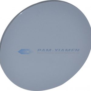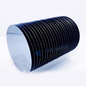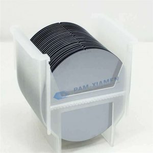
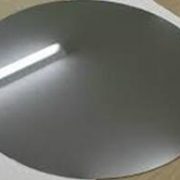
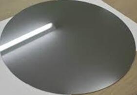
Polierter Wafer
PAM-XIAMEN can offer polished wafer, n type or p type with orientation at <100>, <110> or <111>. FZ polished wafers, mainly for the production of silicon rectifier (SR), silicon controlled rectifier (SCR), Giant Transistor (GTR), thyristor (GRO)
- Beschreibung
Produktbeschreibung
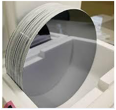
Polierte Waffel
PAM-XIAMEN can offer polished wafer, n type or p type with orientation at <100>, <110> or <111>. More Specifications, please see tables below.
Unsere Vorteile auf einen Blick
- Advanced epitaxy growth equipment and test equipment.
- Offer the highest quality with low defect density and good surface roughness.
- Strong research team support and technology support for our customers
1. Specifications of Polished Silicon Wafers
1.1 FZ Polished Wafers Specifications
FZ polished silicon wafer: mainly for the production of silicon rectifier (SR), silicon controlled rectifier (SCR), Giant Transistor (GTR), thyristor (GRO)
| Typ | Leitungsart | Orientierung | Durchmesser Umfang (mm) | Widerstandsbereich (Ω cm) | Geometrische Parameter Körnigkeit, Oberflächenmetall |
| FZ | N & P. | <100> & <111> | 76.2-200 | >1000 | T≥260 (um) TTV ≤ 2 (um) TIR ≤ 2 (um) STIR ≤ 1 (um) (20 * 20) Graininess≤10pcs(≥0.3um) , ≤20pcs(≥ urface metal≤5E10/cm2 BSD:Etchpit density>1E106pcs/cm2 Poly:5000-12000 A |
| NTDFZ | N | <100> & <111> | 76.2-200 | 30-800 | |
| CFZ | N & P. | <100> & <111> | 76.2-200 | 1-50 | |
| GDFZ | N & P. | <100> & <111> | 76.2-200 | 0.001-300 |
1.2 CZ Polished Wafers Specifications
| Typ | Leitungsart | Orientierung | Durchmesser Umfang (mm) | Widerstandsbereich (Ω cm) | Geometrische Parameter Körnigkeit, Oberflächenmetall |
| MCZ | N & P. | <100> <110> & <111> | 76.2-200 | 1-300 | T≥260 (um) TTV ≤ 2 (um) TIR ≤ 2 (um) STIR ≤ 1 (um) (20 * 20) Graininess≤10pcs(≥0.3um) ,≤20pcs(≥0.2um) Surface metal≤5E10/cm2 BSD:Etchpit density>1E106pcs/cm2LTO:3500~8000±250A |
| CZ | N & P. | <100> <110> & <111> | 76.2-200 | 1-300 | |
| MCZ stark dotiert | N & P. | <100> & <111> | 76.2-200 | 0.001-1 |
2. About Polished Wafer
High-purity electronic grade polysilicon undergoes the steps of crystal pulling, slicing, beveling, lapping, etching, polishing, and cleaning to produce a polished wafer, which meets electrical, surface physical properties, impurity standards and other specifications. Wafers with special processes such as annealing, epitaxy, and SOI are processed based on polished wafers.
Polished wafer (PW) is a silicon chip with atomic flatness that is single side or double sides polished silicon wafer, accounting for about 70% of silicon wafer applications. After the monocrystalline silicon ingot is produced, it is cut into thin slices from the cylindrical monocrystalline silicon of the ingot, which is a wafer of high-purity silicon element. The purpose of polishing is to further remove the residual damage layer on the processed surface. The polished monocrystalline silicon wafer can be directly used to fabricate devices or as an epitaxial substrate material. Polished Si wafer is widely used in digital and analog integrated circuits, memory, power devices and other chips.
N Type Sb Doped Silicon Wafer for Integrated Circuit Manufacturing
PAM XIAMEN offers MCZ silicon ingot and silicon wafer.
PAM XIAMEN bietet schwarze Lithium-Niobat-Wafer für Optiken und SAW-Komponenten an
Stöchiometrisches LPCVD-Nitrid auf Siliziumwafern
4″ Prime CZ Si-Wafer mit einseitig gesputterter Cr/Au-Schichtdicke 10/50 nm
Si-Wafer-Durchmesser ohne Beugung 32 mm für XRD-Messungen
Siliziumnitrid-Wellenleiter - Substrate und bereitgestellte Dienstleistungen
Super Low Stress Nitron auf Siliziumwafern
Nitrid-Siliziumwafer mit geringer Spannung
Siliziumwafer mit (211) -Orientierung
Eigenschaften des Siliziumwafers
Siliziumwafer für die weiche Lithographie
Silicon Fluidic PDMS Micro-Fluidic Chip-Plattformen
Ultra-Verdünnte Silizium-Wafer
Kundenspezifische Siliziumwafer
Dicke des Siliziumwafers: 275 + - 25 um
Dicke des Siliziumwafers: 1000 μm
2 "Siliziumwafer Dicke: 1000 ± 25 μm
Dicke des Si-Wafers: 675 ± 25 um
4 "Si-Wafer Dicke: 500 ± 20 μm
3 "Si-Wafer Dicke: 380 ± 20 μm
50,8 mm (2 Zoll) Siliziumwafer-1
50,8 mm (2 Zoll) Siliziumwafer-2
50,8 mm (2 Zoll) Siliziumwafer-3
50,8 mm (2 Zoll) Siliziumwafer-4
50,8 mm (2 Zoll) Siliziumwafer-5
76,2 mm (3 Zoll) Siliziumwafer
100 mm (4 Zoll) Siliziumwafer-1
100 mm (4 Zoll) Siliziumwafer-2
100 mm (4 Zoll) Siliziumwafer-3
100 mm (4 Zoll) Siliziumwafer-4
100 mm (4 Zoll) Siliziumwafer-5
100 mm (4 Zoll) Siliziumwafer-6
150 mm (6 Inch) Silizium-Wafer
(100) Orientierte Siliziumwafer-1
(100) Orientierte Siliziumwafer-2
(100) Orientierte Siliziumwafer-3
(100) Orientierte Siliziumwafer-4
(100) Orientierte Siliziumwafer-5
(112) Orientierungssiliciumwafer
4″ FZ Intrinsic Silicon Wafer SSP
Sie können auch mögen ...
-
Freistehenden GaN-Substrat
PAM-XIAMEN has established the manufacturing technology for freestanding (gallium nitride)GaN substrate wafer, which is for UHB-LED and LD. Grown by hydride vapour phase epitaxy (HVPE) technology,Our GaN substrate has low defect density.
-
Siliziumepitaxialwafers
Silicon Epitaxial Wafer(Epi Wafer) is a layer of epitaxial silicon single crystal deposited onto a single crystal silicon wafer(note: it is available to grow a layer of poly crystalline Silicon layer on top of a highly doped Singly crystalline silicon wafer, but it needs buffer layer (such as oxide or poly-Si) in between the bulk Si substrate and the top epitaxial silicon layer. It also can be used for thin film transistor.
-
Test-Wafer-Monitor Wafer Dummy-Wafer
Als Dummy-Wafer-Hersteller bietet PAM-XIAMEN Silikon-Dummy-Wafer/Test-Wafer/Monitor-Wafer an, die in einem Produktionsgerät verwendet werden, um die Sicherheit zu Beginn des Produktionsprozesses zu verbessern und zur Lieferkontrolle und Bewertung der Prozessform verwendet werden. Da für Experimente und Tests häufig Dummy-Siliziumwafer verwendet werden, sind Größe und Dicke in den meisten Fällen wichtige Faktoren. Es sind 100 mm, 150 mm, 200 mm oder 300 mm Dummy-Wafer erhältlich.
-
Cz monokristallinem Silizium
PAM-XIAMEN, a monocrystalline bulk silicon producer, can offer <100>, <110> and <111> monocrystalline silicon wafers with N&P dopant in 76.2~200 mm, which are grown by CZ method. The Czochralski method is a crystal growth method, referred to as the CZ method. It is integrated in a straight-tube heat system, heated by graphite resistance, melts the polysilicon contained in a high-purity quartz crucible, and then inserts the seed crystal into the surface of the melt for welding. After that, the rotating seed crystal is lowered and melted. The body is infiltrated and touched, gradually raised, and finished or pulled through the steps of necking, necking, shouldering, equal diameter control, and finishing.
-
Ätzen Wafer
The etching silicon wafers offered by PAM-XIAMEN are N type or P type etching wafers, which have low roughness, low reflectivity and high reflectivity. The etching wafer has the characteristics of low roughness, good glossiness and relatively low cost, and directly substitutes the polished wafer or epitaxial wafer which has relatively high cost to produce the electronic elements in some fields, reducing the costs.
-
SiC-Wafer-Substrat
The company has a complete SiC(silicon carbide) wafer substrate production line integrating crystal growth, crystal processing, wafer processing, polishing, cleaning and testing. Nowadays we supply commercial 4H and 6H SiC wafers with semi insulation and conductivity in on-axis or off-axis, available size:5x5mm2,10x10mm2, 2”,3”,4”, 6” and 8″, breaking through key technologies such as defect suppression, seed crystal processing and rapid growth, promoting basic research and development related to silicon carbide epitaxy, devices, etc.
-
GaAs (Gallium-Arsenid) -Wafer
As a leading GaAs substrate supplier, PAM-XIAMEN manufactures Epi-ready GaAs(Gallium Arsenide) Wafer Substrate including semi-conducting n type, semi-conductor C doped and p type with prime grade and dummy grade. The GaAs substrate resistivity depends on dopants, Si doped or Zn doped is (0.001~0.009) ohm.cm, C doped one is >=1E7 ohm.cm. The GaAs wafer crystal orientation should be (100) and (111). For (100) orientation, it can be 2°/6°/15° off. The EPD of GaAs wafer normally is <5000/cm2 for LED or <500/cm2 for LD or microelectronics.
-
Float-Zone monokristallinem Silizium
PAM-XIAMEN kann Float-Zone-Siliziumwafer anbieten, die nach dem Float-Zone-Verfahren hergestellt werden. Monokristalline Siliziumstäbe werden durch Wachstum in der Floatzone gewonnen und anschließend werden die monokristallinen Siliziumstäbe zu Siliziumwafern verarbeitet, die als Floatzonen-Siliziumwafer bezeichnet werden. Da der zonengeschmolzene Siliziumwafer während des Schwebezonen-Siliziumprozesses keinen Kontakt mit dem Quarztiegel hat, befindet sich das Siliziummaterial in einem suspendierten Zustand. Dadurch wird es während des Schwebezonenschmelzprozesses von Silizium weniger verschmutzt. Der Kohlenstoffgehalt und der Sauerstoffgehalt sind geringer, die Verunreinigungen sind geringer und der spezifische Widerstand ist höher. Es eignet sich für die Herstellung von Leistungsgeräten und bestimmten elektronischen Hochspannungsgeräten.


Related Products
-
12 "Silicon Wafer 300mm TOX (Si Thermische Oxidation Wafer)
PAM-XIAMEN bietet 300-mm-Siliziumoxid-Wafer und Dioxid-Wafer an. Thermooxid-Siliziumwafer oder Siliziumdioxidwafer ist ein blanker Siliziumwafer mit einer Oxidschicht, die durch Trocken- oder Nassoxidationsverfahren gewachsen ist. Die thermische Oxidschicht des Siliziumwafers wird normalerweise in einem horizontalen Rohrofen gezüchtet, und der Temperaturbereich des Siliziumwaferoxids liegt im Allgemeinen zwischen 900 °C und 1200 °C. Im Vergleich zur CVD-Oxidschicht weist die Siliziumwafer-Oxidschicht eine höhere Gleichmäßigkeit, bessere Kompaktheit, höhere Durchschlagsfestigkeit und bessere Qualität auf.
-
12 "Prime Grade Silicon Wafer
PAM-XIAMEN bietet blanke 300-mm-Siliziumwafer (12 Zoll) in erstklassiger Qualität, n-Typ oder p-Typ, und die 300-mm-Siliziumwaferdicke beträgt 775 ± 15. Im Vergleich zu anderen Siliziumwafer-Anbietern ist der Preis für Siliziumwafer von Powerway Wafer wettbewerbsfähiger und die Qualität höher. 300-mm-Siliziumwafer haben eine höhere Ausbeute pro Wafer als durchlässige Siliziumwafer mit großem Durchmesser.
-
12 "Test Grade Silicon Wafer
PAM-XIAMEN bietet 300-mm-Siliziumwafer-Dummys (12 Zoll) in Testqualität, n-Typ oder p-Typ an. Im Vergleich zu anderen Siliziumwafer-Anbietern bietet Powerway Wafer professionellen Service zu wettbewerbsfähigen Preisen.