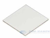
CVD diamond substrate film is available with a maximum working temperature at 600℃ from PAM-XIAMEN at below spec. Single crystal diamond material has the highest thermal conductivity among natural substances known at present. Diamond substrate has stable chemical properties, good electrical insulation and low dielectric constant. The thermal expansion coefficient of diamond substrate is basically the same as that of the device material, and the surface smoothness is good. Currently, diamond substrate wafer is the most ideal material for heat dissipation components of high-end devices with high power density.

1. Synthetic Diamond Substrate Specifications
Diamond Substrate (PAM-190906-Diamond)
Size:
Option 1: 2×2.5 mm;
Option 2: 4×4.5 mm;
Thickness: 0.15+/-0.05mm
Backside polished, Ra<0.03nm,
Front side lapping, Ra<0.25um
Single peak level <= 5nm
Thermal conductivity: 1800w/m.k;
Application: substrates will be mounted under chip crystals as temperature compensators
2. How is the surface treated of CVD diamond substrate?
It depends on the application, usually for the heat sink, it is treated in this way: Bottom surface polishing, growth surface grinding.
When diamond is used as a wafer-level substrate, its surface roughness ra is required to be less than 3nm, and it has a sub-micron-level surface accuracy. When diamond is used as a heat sink for circuit components, it is required to have extremely low surface roughness and extremely high surface accuracy, thereby increasing the contact area and improving the heat dissipation efficiency. In short, these two applications require the single crystal diamond wafer surface to be ultra-smooth, ultra-flat and defect-free.
According to different industrial application requirements, CVD diamond substrate surface polishing technology has become a crucial process link in diamond application. According to market research, the surface roughness required as a heat sink product is about 10 nanometers, while as a substrate, it is less than 1 nanometer. In addition, the expansion of the diameter of the substrate is also a key factor for the successful application of diamond to the preparation and industrialization of power devices. The larger the diameter of the substrate, the greater the number of devices on a single substrate, which can reduce device costs and improve device manufacturing efficiency. Therefore, the polishing of diamond gradually develops in the direction of large size, ultra-smooth, and no damage.
3. Diamand Wafer Substrate Preparation Method
So far, the single crystal diamond substrate growth methods are mainly divided into high temperature and high pressure method (HTHP) and chemical vapor deposition (CVD). The CVD diamond growth method is subdivided into microwave plasma chemical vapor deposition (MP-CVD), radio frequency plasma chemistry Vapor deposition method (RF-CVD) and DC arc plasma jet CVD method. Among all the CVD methods, the MP-CVD technology is recognized as the only one that can realize the preparation of high-quality semiconductor single crystal diamond substrate and epitaxial wafer materials. The maximum size of single non-spliced homoepitaxial single crystal diamond substrates currently reported is 10mm×10mm. The appearance and composition of CVD diamond thin film are almost the same as natural diamond. Moreover, the physical and chemical properties of the CVD diamond are not much different. Compared with natural diamond, the CVD diamond substrate semiconductor material is more cleaner and has almost no impurities.
Generally, the device structure is not directly prepared on the diamond film, but a thin (generally in the order of micrometers) high-quality epitaxial structure is grown on the substrate. The high-quality epitaxial structure is used as the functional layer of the device, and the substrate of diamond by CVD plays a supporting role for the epitaxial growth.
More about how to make diamond wafer, please watch: https://youtu.be/XQEFCeY06Do
4. CVD Single Crystal Diamond Sheet Applications
The large single crystal diamond material grown by CVD method can be used as a diamond substrate semiconductor for integrated circuit chips, ultra-high-frequency high-power electronic devices, biosensors, aerospace and other extreme environment electronic components, etc., which will greatly improve data transmission speed and conversion efficiency, reduce power consumption. In the near future, the CVD diamond single crystal substrate plays a strategic role in many fields, such as aerospace, energy exploration, quantum computers, optical storage, 5G communications, solar energy, automobile manufacturing, semiconductor lighting, and smart grids.

For more information, please contact us email at victorchan@powerwaywafer.com and powerwaymaterial@gmail.com.
