Diamond wafers from PAM-XIAMEN are wafer-scale products that are used to tap the huge potential of diamond materials, such as tribological testing, unique nano-scale processing applications and MEMS development. In the current diamond wafer market, there are three grade diamond wafer, Microelectronics Grade diamond wafer, Thermal Grade diamand wafers and slices and Optical Grade diamond wafers:
1. Microelectronics Grade Diamond Wafer for Wafer Fabrication
The wafers can be done experiment with the remarkable properties of diamond, and the specifications, like performance consistency, bow and thickness, meet those of baseline wafer-level, which can make the diamond wire wafer slicing insert directly into the MEMS foundry process.
The composite substrate prepared by the thin diamond film/heterogeneous substrate not only has the high thermal conductivity performance of diamond, but also reduces the cost of the thick diamond film, which can be directly used for epitaxial substrate of wide band gap semiconductor material and the growth of materials. The heat dissipation factor is directly considered from the epitaxial material itself, which is also a major development direction for semiconductor devices in the future. The semiconductor wafer materials are all developing in the large-size wafers, which requires that the diamond single crystal wafer material must be large size and high quality. At the same time, the excellent heat dissipation performance can make a better performance of the device.
1.1 Specification of Microelectronics Grade Diamond Wafer
No. 1 Polycrystalline Diamond Wafer
| Diamond Wafer | Polycrystalline Diamond |
| Growth Method | MPCVD |
| Wafer Thickness | 0~500um+/-25um |
| Wafer Size | 1cm*1cm;2inch; custom |
| Surface Roughness | Ra< 1 nm |
| FWHM (D111) | 0.354 |
| Coefficient of Thermal Expansion | 1.3×10^-6 K^-1 |
| Thermal conductivity | >1000 W/m.K |
| Item | Wafer Scale Diamond | |
| Thickness | 100um | 300um |
| Growth method | MPCVD | MPCVD |
| Size | 2 inch | 2 inch |
| Surface roughness of growth surface | <1nm Ra | <1nm Ra |
| Warp | 50um | 30um |
| FWHM (D111) | 0.354 (D111) | 0.354 (D111) |
| Thermal expansion coefficient | 1.3 (10-6K-1) | 1.3 (10-6K-1) |
| Thermal conductivity (T.C)
TDTR Detection method |
1500±200 W/mK
(13 scans with different spot size) |
1500±200 W/mK
(13 scans with different spot size) |
![]()
1.2 Manufacturing Flow of Microelectronics Grade Diamond Wafer
![]()
1.3 XRD Spectra of 2inch CVD Diamond Wafer
The primary crystal facets orientation of CVD diamond films is (111) plane.
![]()
1.4 Raman Spectra of 2inch CVD Diamond Wafer
There is only one single diamond peak at 1333.48 cm-1.
![]()
1.5 SEM Micrographs( × 1k) of the 2-inch Diamond Wafer after Rough Polishing
![]()
1.6 AFM Micrographs of the 2-inch Diamond Wafer after Rough Polishing
Image Ra = 137 nm with the scanning area of 5×5 μm2.
![]()
1.7 SEM Micrographs(× 1k) of the 2-inch Polycrystalline Diamond Wafer after Finishing Polishing
![]()
1.8 AFM Micrographs of the 2-inch Diamond Wafer after Finishing Polishing
Image Ra = 0.278 nm with the scanning area of5×5 μm2.
![]()
Image Ra = 0.466 nm with the scanning area of 15×15 μm2.
![]()
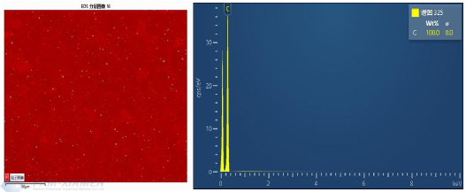
1.9 EDS Results for Polished Films
The content of elements on the polished area is all carbon. No metal contamination from the polishing plate.
1.10 XPS Results for Polished Films
![]()
2. Thermal Grade Diamand Wafers and Slices
Diamond exhibits the highest thermal conductivity among all materials. Its thermal conductivity is up to 2000 W/mK which is higher a lot than that of copper. Therefore, diamond wire cut wafer and slice become more and more popular in thermal management as heatspreaders, heatsinks, lithographically patterned metallization, electrical isolation between top and bottom metallization, stress relieving slits for stress free mounting etc.
CVD diamond heat spreaders in various shapes,and the typical parameters are as follows:
| Item | Value |
| Diameter | 80mm, or small size such as 5*5mm2 |
| Available Thickness | 0.3mm |
| Thickness tolerance | ﹢/-0.02mm |
| Process | DC Arc Plasma |
| Structure | Polycrystalline |
| Chemical composition | 100% C |
| Density | 3.52 g/cm³ |
| Poisson’s ratio | 0.1 |
| Young’s modulus | 1000-1100 Gpa |
| Thermal conductivity | C>1,000 W/m.K, B>1300W/m.K,A>1800W/m.K |
| Tensile strength | >350 kg/mm² |
| Vickers Hardness | 7000~10000 kg/mm² |
| Compressive strength | >110GPa |
| Thermal stability | 800℃ |
| Wear resistance(abrasion ratio) | 100,000~200,000 |
| Chemical Stability | Insoluble in alkali and acid |
| Surface finish polished | <50 nm |
| Surface finish lapped | <0.5 um |
3. Optical Grade Diamond Wafer
Optical grade diamond wafers are used as window for infrared beam splitters, lenses for terahertz spectroscopy and CO2 laser surgery, Brewster Windows for multi-spectral applications such as free electron lasers, multi-wavelength IR lasers or terahertz optical systems, for Units attenuated total reflection) spectroscopy, for diamond Liquid Cells. Below is the datasheet of the diamond wafer in optical level for your reference:
| Parameter | Optical Grade Diamond Wafer | ||
| Size | (3~50)±1 mm | ||
| Thickness | (100~600)±30 um | ||
| Surface Process | Polished both sides | ||
| Roughness | A<5 nm | B<10 nm | C<30 nm |
Following diagram shows the optical grade diamond substrate transmission rate:

Transmission Rate of Diamond Wafer
Source:PAM-XIAMEN

For more information, please contact us email at victorchan@powerwaywafer.com and powerwaymaterial@gmail.com