The wide band gap semiconductor materials represented by GaN and SiC have the advantages of fast electron saturation drift and strong radiation resistance, and have a wide range of applications in solid-state lighting, electronic power and mobile communications. Among them, solid-state lighting is of great significance for improving today’s global warming and the deterioration of the ecological environment. In addition to energy saving and environmental protection, UV LEDs represented by deep ultraviolet light-emitting diodes (DUV LEDs) have been widely used in sterilization and disinfection fields due to their large photon energy. As a leading wafer manufacturer, PAM-XIAMEN provides AlGaN / GaN epitaxial wafers for LED fabrication, please refer to https://www.powerwaywafer.com/gan-wafer/epitaxial-wafer.html for specific structures.
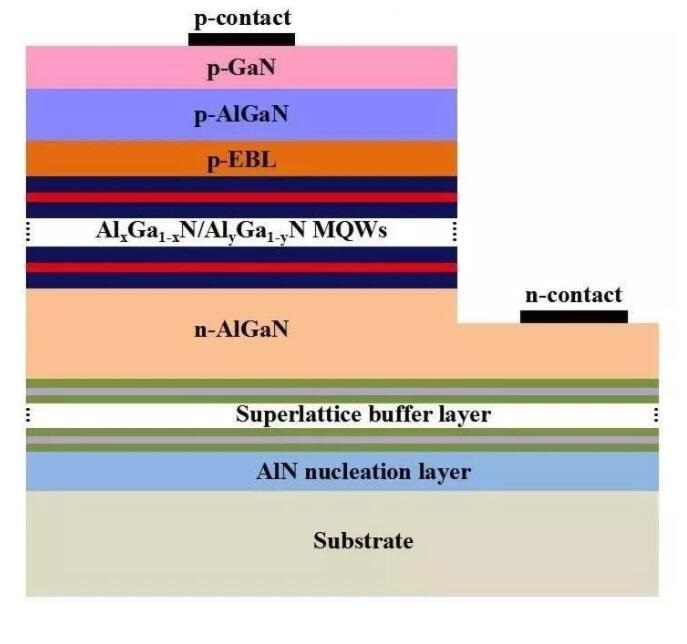
Fig.1 Typical Epitaxial Structure of DUV LED Device
UV LEDs can be subdivided into: UVA LEDs (320 nm<λ<400 nm), UVB LEDs (280 nm<λ<320 nm), UVC LEDs (200 nm<λ<280 nm) and VUV (10 nm) <λ<200 nm), where the emission wavelength of DUV LED is shorter than 360 nm. The AlGaN material has the characteristics of direct band gap and adjustable band gap (3.4 eV~6.2 eV), covering most of the ultraviolet emission band (200 nm ~ 365 nm), so it becomes an ideal material for the preparation of DUV LEDs. We can supply UV LED epi wafer with wavelength of 275nm~405nm, specification please see https://www.powerwaywafer.com/uv-led-wafer-2.html. In recent years, thanks to the more perfect preparation technology of AlGaN materials, DUV LEDs have also made great progress and development.
However, DUV LEDs based on AlGaN materials still face many problems. Among them, the low carrier injection efficiency limits the device performance of DUV LEDs, especially the hole injection efficiency. On the one hand, with the increase of Al composition, the ionization energy of Mg impurity gradually increases, resulting in extremely low ionization rate of Mg; the mobility of the source region, especially the holes, is relatively low.
In addition, low hole concentration and low hole mobility will cause the current to crowd mainly under the electrode, causing the current crowding effect. As a result, the local concentration of carriers is increased, the Auger recombination probability in the active region is increased, the junction temperature of the device is increased, and the service life of the DUV LED is affected.
So, how to solve this problem? We share several solutions with you.
In view of the low hole injection efficiency in DUV LED devices, the researchers optimized the structure of DUV LED devices, and proposed the concept of dielectrically regulated tunneling junction, electric field memory, p-AlyGa1-yN/p-AlxGa1-xN/p-AlyGa1-yN (x<y) EBL and other measures to improve hole injection efficiency. Specifically as follows:
1. Dielectrically Regulated Tunneling Junction
The p-type electrode of traditional LED is directly sputtered and evaporated on the p-type semiconductor layer, and the low Mg doping efficiency leads to an obvious hole depletion region in the p-type semiconductor layer, which increases the operating voltage of the device and reduces hole concentration in the supply layer.
To this end, the researchers propose to use traditional homogenous tunneling junctions (p+-GaN/n+-GaN) and polarized tunneling junctions (p+-GaN/InGaN/n+-GaN), in which the n+-GaN layer is used as the metal contact layer, improving the hole injection and electrical properties of LED devices. For UV LEDs, the InGaN intercalation layer has serious light absorption for photons in the ultraviolet band.
At the same time, considering that the relative permittivity of AlGaN material decreases with the increase of AlN composition, as shown in Figure 2(a), certain research team used AlGaN material as the insertion layer, and proposed the concept of dielectrically regulated tunnel junction. The enhanced junction electric field increases the electron tunneling probability, thereby increasing the non-equilibrium hole concentration in the p+-GaN layer.
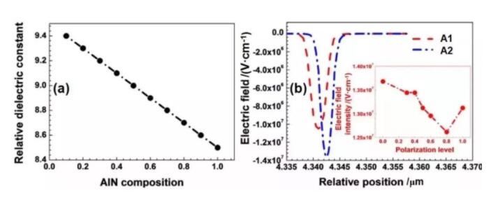
Fig. 2 (a) The relationship between the relative permittivity and AlN composition of the AlxGa1-xN layer; (b) the device with conventional homogeneous tunneling junction (A1) and the device with dielectric tunable tunneling junction (A2) electric field distribution in the tunnel junction region. The inset shows the relationship between the peak electric field and polarization level in the tunnel junction region.
2. Electric Field Memory
The hole supply layer of the conventional DUV LED device includes two parts, a p-AlGaN layer and a p-GaN layer. At the interface between the two, there is a barrier height (i.e. Φh) that prevents holes from being injected from the p-GaN layer to the p-AlGaN layer, so a hole depletion region is generated near the p-AlGaN layer near the p-GaN layer, such as Figure 3(a), and the width of the depletion region increases with Φh, causing the holes to be severely depleted in the p-AlGaN layer.
In response to this problem, researchers found that the direction of the depletion electric field is consistent with the direction of hole transport, which can accelerate holes to a certain extent and increase the ability of holes to be injected into the active region, as shown in Figure 3(b). Φh ensures that the depletion electric field in the p-AlGaN layer is not shielded by free carriers. So the research team came up with the concept of an electric field memory, in which holes can continuously harvest energy from this depleting electric field.
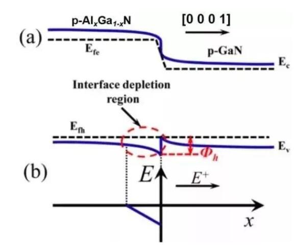
Fig. 3 (a) The corresponding energy band diagram of the hole supply layer p-AlxGa1-xN/p-GaN heterojunction of the DUV LED device, in which the p-AlxGa1-xN layer has an interfacial depletion region; (b) Schematic diagram of the electric field direction in the depletion region at the interface of the p-AlxGa1-xN layer.
3. p-AlyGa1-yN/p-AlxGa1-xN/p-AlyGa1-yN (x<y) EBL
p-EBL prevents electron leakage and also hinders hole injection into the active region. Figure 4(a) shows that a large number of holes will accumulate at the p-EBL/p-AlGaN interface, and only a few holes with high energy are injected into the active region through the thermal radiation mechanism (i.e. P1).
Inserting a thin layer of low-bandwidth material near the p-AlGaN layer in the EBL is suggested. The accumulation of holes at the p-EBL/p-AlGaN interface is reduced by the in-band tunneling mechanism (i.e. P0), and then the holes are injected into the active region through the thermal radiation mechanism (P2), as shown in Figures 4(b), 4(c).
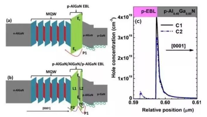
Fig. 4 (a) energy band diagram of conventional DUV LED device; (b) energy band diagram of DUV LED device with p-AlxGa1-xN/AlyGa1-yN/AlxGa1-xN (x>y) EBL; (c) hole distribution maps of p-EBL and p-AlGaN layers.
4. Increase Polarization Effect on Hole Injection
III-V nitrides have an important physical property, the polarization effect. For the traditional [0001] crystal orientation DUV LED, the polarization effect not only leads to the quantum confinement Stark effect, but also seriously affects the carrier injection efficiency, resulting in the degradation of device performance. However, when the polarization level of the DUV LED device structure was changed as a whole, the performance of the device with the [0001] crystallographic orientation (polarization level greater than 0) was significantly better than that of the [000-1] crystallographic orientation, and the optical output power increased with the polarization level increased and further improved. Figures 5(a) and 5(b) show that under different polarization levels, the distribution of holes in the active region, p-EBL and hole supply layer is quite different.
This phenomenon is studied, and it is found that increasing the polarization level at the p-EBL/p-AlGaN/p-GaN interface increases the energy of holes on the one hand, and weakens the barrier height of p-EBL to holes on the other hand, thereby improving the hole injection efficiency and improving the device performance of the DUV LED.
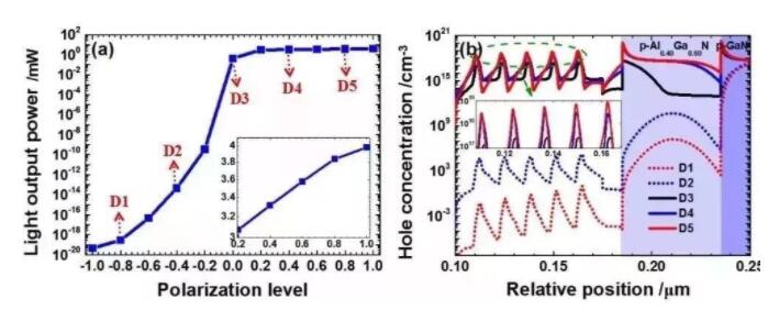
Fig. 5 when the injection current is 35mA, (a) the relationship between the optical output power and the polarization level of the DUV LED device; (b) distribution of holes in quantum wells, p-AlGaN layers and p-GaN layers at different polarization levels
5. Increasing AlN Composition of Quantum Barrier Improves Hole Injection
It’s also found that the last quantum barrier and the polarized charge at the p-EBL interface have important effects on the hole injection efficiency. When the quantum barrier composition is appropriately increased (E3>E2>E1), the electron concentration in the quantum well increases significantly, which is mainly because the quantum barrier’s ability to bind electrons is enhanced. Similarly, the blocking effect of the quantum barrier on holes will also be significantly enhanced, which is theoretically unfavorable for the injection of holes. But the research result shows that the holes increase with the increase of the quantum barrier composition. This is because with the increase of AlN composition in the quantum barrier, the polarization mismatch between the last quantum barrier and p-EBL decreases, which weakens the blocking ability of p-EBL to holes, thereby improving the active region, see figure 6(c).
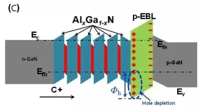
Fig. 6 (c) Schematic diagram of energy band of UVA LED device
In addition to seeking breakthroughs in epitaxial growth technology, understanding the internal physical mechanism of DUV LEDs will help researchers in the field to better understand DUV LEDs and improve the performance of DUV LED devices.

For more information, please contact us email at victorchan@powerwaywafer.com and powerwaymaterial@gmail.com.