With the continuous progress of semiconductor technology, semiconductor devices such as LEDs, photovoltaic cells, semiconductor lasers, etc. have been widely used in people’s daily life and work. In order to ensure the quality and cost control in the production process of the semiconductor device, it is generally necessary to perform various on-line performance tests on the semiconductor device in the production process. Taking LED as an example, in the LED manufacturing process, it is usually necessary to perform electroluminescence (EL) testing on the LED epitaxial wafer.
To ensure the performance of the LED wafers offered by us (more wafer specifications please view: https://www.powerwaywafer.com/gan-wafer/epitaxial-wafer.html), we will test the wafer performance after it made. Below we describe the electroluminescence testing techniques performed on our GaAs LED wafers:
1. GaAs-based Red LED Wafer for EL Testing
| Structure | Thickness (nm) |
| C-GaP | – |
| Mg-GaP | – |
| Mg-AlGaInP (transitional layer) | – |
| Mg-AlInP | – |
| AlInP | – |
| MQW: AlGaInP | – |
| Si-AlInP | – |
| Si-Al0.6GaInP | – |
| Si-GaInP | 8.8 |
| Si-GaAs (ohm contact layer) | – |
| Si-GaInP (etched layer) | – |
| Si-GaAs (buffer layer) | – |
| GaAs substrate |
2. What is Electroluminescence?
Electroluminescence is also called field luminescence. At present, electroluminescence imaging technology has been used by many solar cell and module manufacturers to detect potential defects of products and control product quality.
As for LED electroluminescence film, electroluminescence spectroscopy is an important technique for characterizing new LEDs and facilitating their development. The performance of light-emitting devices can be studied by electroluminescence and time-resolved spectroscopy. According to the emission spectrum, the chromaticity coordinates and color rendering index of the LED, as well as the basic properties such as the band gap of the semiconductor can be calculated.
3. How to Do the Electroluminescence Testing?
EL measurements are usually performed on finished devices (such as LEDs) because it requires a device structure to inject current. The electroluminescence testing tool applies a forward current of 1-40mA to the cell, acting on both sides of the diffusion junction, and the electric energy excites the atoms in the ground state, making them in the excited state, and the atoms in the excited state are unstable and carry out spontaneous radiation. Through the function of the filter and the exposure degree of the film to understand the intrinsic transition in the spontaneous emission; through the relationship between minority carrier lifetime, density and light intensity, from the exposure degree of the film, to judge whether there is a defect on GaAs LED epi wafer.
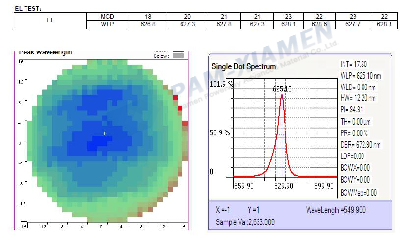
When do the El test for the above LED wafer, we test in the middle of the wafer, select several points, and then test at 20mA current. The electroluminescence data we tested are shown as figure below:
4. FAQ for GaAs LED Wafer
Q: How do you typically make contact to the GaP:C p-contact layer of GaAs LED wafer? For example, ITO or Ti/Pt/Au?
A: Usually we make ITO as contact for GaAs LED epitaxy.
Remark:
The Chinese government has announced new limits on the exportation of Gallium materials (such as GaAs, GaN, Ga2O3, GaP, InGaAs, and GaSb) and Germanium materials used to make semiconductor chips. Starting from August 1, 2023, exporting these materials is only allowed if we obtains a license from the Chinese Ministry of Commerce. Hope for your understanding and cooperation!

For more information, please contact us email at victorchan@powerwaywafer.com and powerwaymaterial@gmail.com.