
Research on the Epitaxial Growth of 3C-SiC on 4H-SiC Substrates +
PAM-XIAMEN is capable of providing 3C-SiC substrates and epi-wafers. For details, please contact: [email protected]
Silicon carbide (SiC), due to its high critical breakdown electric field, high thermal conductivity, excellent temperature stability, and chemical inertness, exhibits great potential for applications in high-temperature, high-power electronic devices. SiC exists in various crystalline forms (polytypes). Among them, cubic 3C-SiC possesses the smallest bandgap (2.3eV) and lacks spontaneous polarization effects, making it suitable as a channel material for electronic devices. Unlike traditional heterojunctions (e.g., SiC/Si, AlGaN/GaN), the 3C-SiC/4H-SiC polytype heterojunction offers the advantages of lattice matching and identical chemical composition, which can avoid issues of atomic interdiffusion, making it particularly suitable for devices such as High Electron Mobility Transistors (HEMTs).
However, the epitaxial growth of 3C-SiC still faces numerous challenges, especially concerning defect control. Double positioning boundary (DPB) defects and super-V-shaped structure (SVSS) defects are the main factors affecting the quality of 3C-SiC epitaxial layers. This article synthesizes several relevant publications to review the research progress on the epitaxial growth methods, defect formation mechanisms, and structural property characterization of 3C-SiC/4H-SiC heterostructures.
1. Epitaxial Growth Methods and Process Optimization for 3C-SiC/4H-SiC
Most studies employ high-temperature chemical vapor deposition (CVD) to epitaxially grow 3C-SiC on 4H-SiC substrates. A typical growth process includes the following steps:
Substrate Pretreatment: In-situ etching from room temperature to 1600°C in an H₂ atmosphere to remove surface scratches and defects.
Homogeneous Epitaxy: 4H-SiC homoepitaxy at 1600°C to form step-bunching, providing a platform for subsequent 3C-SiC nucleation.
Nucleation Stage: Temperature is reduced to 1550°C, and SiH₄ and C₃H₈ are introduced for 3C-SiC nucleation.
Heteroepitaxial Growth: Temperature is further reduced to 1500°C–1580°C for the growth of the 3C-SiC epitaxial layer.
Xin et al. systematically investigated the influence of each step on surface morphology and defects through a four-step experiment, finding that DPB defects under high-temperature conditions exhibited “hillock”-like protrusions rather than traditional shallow grooves.
Researchers like Jiao et al. utilized methyltrichlorosilane (MTS) as a precursor, significantly simplifying the process flow and achieving an ultra-high growth rate of 278μm/h at 1500°C, markedly improving epitaxial efficiency and reducing costs. This study also systematically compared the epitaxial and oxidation behaviors of four sample types: Si-face/n-type, C-face/n-type, Si-face/semi-insulating, and C-face/semi-insulating.
2. Defect Mechanisms and Structural Characterization
2.1 DPB Defects in 3C-SiC on Si-Face 4H-SiC Growth
During 3C-SiC epitaxy on Si-face 4H-SiC, DPB defects form due to the existence of two stacking sequences (3C-I and 3C-II types). Analysis via Transmission Electron Microscopy (TEM) and Selected Area Electron Diffraction (SAED) revealed that DPB defects exhibit a V-shaped structure, composed of incoherent boundaries between two twin regions (Twin-I and Twin-II). Feng et al. proposed a kinetics model based on adatom migration, explaining the linear extension of V-shaped boundaries and the formation mechanism of non-linear DPBs.

Fig. 1 (a) Cross-sectional TEM image of 3C-SiC on Si-face 4H-SiC measured along the [-2110] axis at low magnification; (b), (c), and (d) show SAED patterns obtained from the left, right, and central bottom regions of the epilayer, respectively.
2.2 SVSS and Polycrystalline Composite Defects in 3C-SiC on C-Face 4H-SiC Growth
In 3C-SiC grown on C-face 4H-SiC, super-V-shaped structures (SVSS) and polycrystalline composite defects are frequently observed. SVSS consists of a high protrusion point and two straight arms extending for several millimeters. Its formation is related to the migration of adatoms in the step-flow and anti-step-flow directions. Feng et al. noted that the vertex of an SVSS is typically caused by polycrystalline nucleation, with its arm angles ranging between 50°–90°, depending on growth conditions.

Fig. 2 Optical images of different 3C-SiC epitaxial samples showing SVSS defects
2.3 Surface Morphology and Crystal Quality Analysis of 3C-SiC
Atomic Force Microscopy (AFM) and Scanning Electron Microscopy (SEM) images show that DPB defects on the Si-face present a layered structure with a height of about 0.15μm, while polycrystalline nucleation defects on the C-face exhibit island-like structures with heights up to 1.75μm. X-ray Diffraction (XRD) and Raman spectroscopy analysis indicate that the crystalline quality of Si-face epilayers is superior to that of C-face epilayers, where polycrystalline nucleation leads to disordered crystal arrangement.
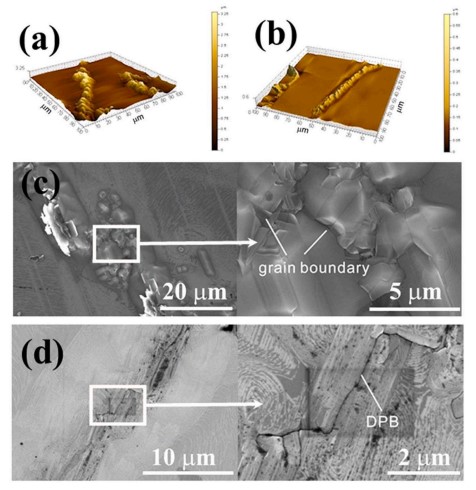
Fig. 3 AFM images of 3C-SiC films on (a) C-face and (b) Si-face 4H-SiC substrates; Schematic SEM morphology for (c) C-face and (d) Si-face
3. Influence of Growth Temperature on the Properties of 3C-SiC Epilayers
Wang et al. systematically studied the impact of growth temperature (1530°C–1580°C) on the properties of 3C-SiC films on 4H-SiC substrates:
XRD Analysis: As temperature decreased from 1580°C to 1550°C, the Full Width at Half Maximum (FWHM) of diffraction peaks and dislocation density gradually decreased, indicating improved crystal quality. Quality degraded upon further reduction to 1530°C.

Fig. 4 XRD patterns of 3C/4H-SiC films grown at different temperatures, measured at room temperature
Raman Spectroscopy: The Transverse Optical (TO) peak position shifted to lower frequency with increasing temperature, indicating changes in lattice stress. Variable-temperature Raman tests showed a redshift of the TO peak position with rising temperature, with peak width influenced by three-phonon and four-phonon processes.

Fig. 5 Raman scattering spectra of 3C/4H-SiC grown at different temperatures, under different laser wavelengths
XPS Analysis: The surface contained chemical bonds such as Si–C, Si–O, C–C, and C–O. High-temperature samples had a thinner surface C–H/C–C layer, suggesting a cleaner surface.

Fig. 6 XPS spectra of 3C/4H-SiC films grown at different epitaxial temperatures
Significant progress has been made in the epitaxial growth technology of 3C-SiC on 4H-SiC substrates, particularly in the optimization of high-temperature CVD processes, understanding of defect mechanisms, and control of crystal quality. Si-face epitaxy is predominantly challenged by DPB defects, while C-face epitaxy mainly contends with SVSS and polycrystalline nucleation. Growth temperature significantly influences the crystal quality, surface state, and optical properties of the epilayers, with 1550°C identified as a relatively optimal temperature. Future research should continue to explore more efficient, low-defect epitaxial processes, combined with interface engineering and post-processing techniques, to further enhance the application potential of 3C-SiC/4H-SiC heterojunctions in power electronic devices.

Whether you need 3C-SiC on 4H-SiC epitaxy for researches, please contact us email at [email protected] and [email protected].
References:
- Xin, B., Jia, R. X., Hu, J. C., Tsai, C. Y., Lin, H. H., & Zhang, Y. M. (2015). A step-by-step experiment of 3C-SiC hetero-epitaxial growth on 4H-SiC by CVD. Applied Surface Science, 357, 985-993.
- Jingyi, J., Zhao, S., Li, Y., Wei, M., Yan, G., & Liu, X. (2024). Ultrahigh growth rate-induced thick 3C-SiC heteroepitaxial layers on 4H-SiC and its oxidation characteristics. Vacuum, 229, 113588.
- Feng, Z. C., Lin, H. H., Xin, B., Tsai, S. J., Saravade, V., Yiin, J., … & Ferguson, I. T. (2023). Structural characteristics of 3C–SiC thin films grown on Si-face and C-face 4H–SiC substrates by high temperature chemical vapor deposition. Vacuum, 207, 111643.
- Wang, B., Yin, J., Chen, D., Long, X., Li, L., Lin, H. H., … & Wan, L. (2021). Optical and surface properties of 3C–SiC thin epitaxial films grown at different temperatures on 4H–SiC substrates. Superlattices and Microstructures, 156, 106960.