Single crystal AlN substrate can be provided with specifications as found in https://www.powerwaywafer.com/aln-substrate.html.
AlN single crystal is the direct bandgap semiconductor material with the largest bandgap width (6.2 eV), which has excellent characteristics such as extremely high breakdown field strength, excellent thermal conductivity, stable physical and [...]
2024-04-18meta-author
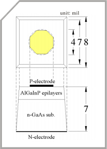
PAM-XIAMEN Offers GaAs LED epitaxy wafer, which is AlGaInP LED (Red LED) stack on GaAs substrate. Xiamen Powerway Advanced Material Co.,Ltd., a leading supplier of GaAs epi wafer and other related products and services announced the new availability of size 2”&4” is on mass production in 2010. This new product [...]
2018-05-14meta-author
GaN(Gallium nitride), which is a compound semiconductor,it is a hard, high melting point materials, the melting point of about 1700 ° C, GaN is a high degree of ionizationof III-Vcompound (0.5 or 0.43). At atmospheric pressure, the GaN crystal is generally hexagonal wurtzite structure. In a cell four atoms, the atomic volume is about halfthat of the GaAs. GaN is Non-Toxic.
Basic Parameters for Wurtzite crystal structure at 300K:
Breakdown field
~5 x 10⁶ V cm-1
Mobility electrons
=< 1000 cm2 V-1 s-1
Mobility holes
=< 200 cm2 V-1 s-1
Diffusion coefficient [...]
2012-05-21meta-author
GaN
PAM XIAMEN offers Coated Silicon wafer.
Nickel <111> Film( 100nm) Coated Si Wafer (100) P/Boron ,10x10x0.5mmSSP, R:1-20 ohm.cm
Nickel <111> Film( 100nm) Coated Si Wafer (100) P/Boron ,5x5x0.5mmSSP, R:1-20 ohm.cm
Nickel<111> Film (100nm) Coated SiO2/Si Wafer -(100) P/Boron ,10x10x0.5mmSSP, R:1-20 ohm.cm
Nickel<111> Film (100nm) [...]
2019-04-28meta-author
New graphene fabrication method uses silicon carbide template
Graphene transistors. Georgia Tech researchers have fabricated an array of 10,000 top-gated graphene transistors, believed to be the largest graphene device density reported so far.
(PhysOrg.com) — Researchers at the Georgia Institute of Technology have developed a new [...]
2018-05-17meta-author
‘Optically pumped’ laser closer to improving processing speed of sensors
Researchers are developing a new material that could improve processing speed of sensors and other electronic components. Credit: University of Arkansas
Imagine creating a material for the digital information highway that allows a fast lane of [...]
2018-02-11meta-author