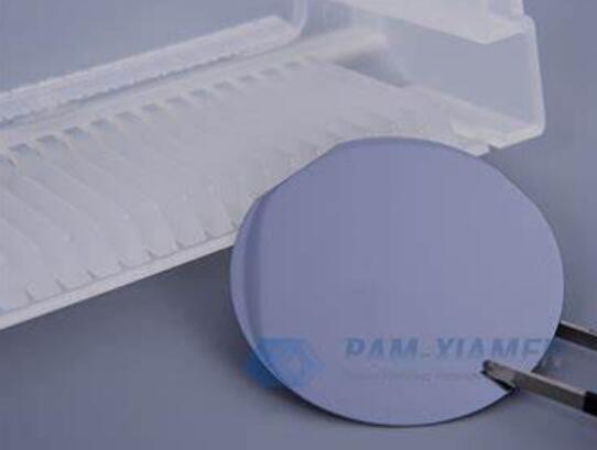
La oblea de fosfuro de indio monocristalino de grado ficticio está disponible con dopaje S cultivado por VGF. La concentración de electrones de la oblea de fosfuro de indio tipo N alcanza 1018cm-3, y la resistividad del fosfuro de indio es muy baja, generalmente 10-2~10-3Ω·cm. It is mostly used in high-speed optoelectronic devices, such as LD, LED, PIN- PD, PIN-APD and etc. EPD map of InP can be offered if necessary, please contact us at victorchan@powerwaywafer.com. The specifications of the test grade InP wafers se enumeran de la siguiente manera:
1. Especificaciones de la oblea de fosfuro de indio en calidad ficticia
Artículo 1:
| Artículo | Parámetro | UOM |
| Materiales | Oblea de fosfuro de indio | |
| Grado | Grado ficticio | |
| Diámetro | 50,0 ± 0,5 | mm |
| Espesor | Mín .: 300 Máx .: 400 | um |
| Orientación | (100) ± 0,5 ° | |
| Tipo de conductividad / Dopante | SCN / S | |
| Longitud plana primaria | 16 ± 2 | mm |
| Orientación plana primaria | EJ (0-1-1) | |
| Secundaria plana Longitud | 7 ± 1 | mm |
| Orientación plana secundaria | EJ (0-11) | |
| concentración de portadores | Mínimo máximo: / | cm-3 |
| Resistividad | Mínimo máximo: / | ohmios-cm |
| Movilidad | Mínimo máximo: / | cm2/ V * seg |
| EPD | Ave: / Max: <1000 cm-2 | cm-2 |
| TTV | 10 | um |
| TIR | 10 | um |
| ARCO | 10 | um |
| Deformación | 15 | um |
| Superficie | P / P, P / E | |
| Redondeo de bordes | 0,25 (conforme a los estándares SEMI) | mmR |
| Listo para Epi | Sí | |
| Marcos láser | / | |
| Área gemela laminar | área de monocristal útil con (100) orientación> 80% | |
| Paquete | recipiente individual lleno de N2 |
Ítem 2:
| Artículo | Parámetro | UOM |
| Materiales | Sustrato de fosfuro de indio | |
| Grado | Grado ficticio | |
| Diámetro | 76,2 ± 0,5 | mm |
| Espesor | Mín .: 600 Máx .: 650 | um |
| Orientación | (100) ± 0,5 ° | |
| Tipo de conductividad / Dopante | SCN / S | |
| Longitud plana primaria | 22 ± 1 | mm |
| Orientación plana primaria | EJ | |
| Secundaria plana Longitud | 12 ± 1 | mm |
| Orientación plana secundaria | EJ | |
| concentración de portadores | Mínimo máximo: / | cm-3 |
| Resistividad | Mínimo máximo: / | ohmios-cm |
| Movilidad | Mínimo máximo: / | cm2/ V * seg |
| EPD | Ave: / Max: <1000 cm-2 | cm-2 |
| TTV | 10 | um |
| TIR | 10 | um |
| ARCO | 10 | um |
| Deformación | 15 | um |
| Superficie | P / P, P / E | |
| Redondeo de bordes | 0,25 (conforme a los estándares SEMI) | mmR |
| Listo para Epi | Sí | |
| Marcos láser | / | |
| Área gemela laminar | área de monocristal útil con (100) orientación> 80% | |
| Paquete | recipiente individual lleno de N2 |
Tema 3:
| Artículo | Parámetro | UOM |
| Materiales | Oblea de fosfuro de indio | |
| Grado | Grado ficticio | |
| Diámetro | 100,0 ± 0,5 | mm |
| Espesor | Mín .: 600 Máx .: 650 | um |
| Orientación | (100) ± 0,5 ° | |
| Tipo de conductividad / Dopante | SCN / S | |
| Longitud plana primaria | 32,5 ± 1 | mm |
| Orientación plana primaria | EJ | |
| Secundaria plana Longitud | 18 ± 1 | mm |
| Orientación plana secundaria | EJ | |
| concentración de portadores | Mínimo máximo: / | cm-3 |
| Resistividad | Mínimo máximo: / | ohmios-cm |
| Movilidad | Mínimo máximo: / | cm2/ V * seg |
| EPD | Ave: / Max: <1000 cm-2 | cm-2 |
| TTV | 10 | um |
| TIR | 10 | um |
| ARCO | 10 | um |
| Deformación | 15 | um |
| Superficie | P / P, P / E | |
| Redondeo de bordes | 0,25 (conforme a los estándares SEMI) | mmR |
| Listo para Epi | Sí | |
| Marcos láser | / | |
| Área gemela laminar | área de monocristal útil con (100) orientación> 80% | |
| Paquete | recipiente individual lleno de N2 |
2. Aplicaciones de fosfuro de indio de grado ficticio
La oblea de InP de grado ficticio se utiliza para la prueba del proceso de crecimiento de epi y la caracterización de la composición en la capa epitaxial. No es adecuado para grabar estructuras de dispositivos, por ejemplo, guías de ondas y rejillas ópticas debido a los cristales gemelos y los posibles orificios de la orientación de la oblea en el lado gemelo.
Microtwin o linaje de la superficie de la oblea <20% es aceptable.
3. Propiedades del fosfuro de indio
Indium phosphide is a group III-V compound semiconductor material compounded by the combination of group III element indium (In) and group V element phosphorus (P). It has a zinc blende structure with a indium phosphide lattice constant of 0.586 9 nm. InP single crystal is soft and brittle, silver-gray with metallic luster. The indium phosphide band gap at room temperature is 1.344 eV, which is a direct transition band structure. The emission wavelength is 0.92 um, the intrinsic carrier concentration of InP at room temperature is 2×107cm-3, y la movilidad de electrones y huecos son 4500 cm2/ Vs y 150 cm2 / V · s respectivamente.

Estructura cristalina de fosfuro de indio
4. Proceso de fabricación de obleas InP
El fosfuro de indio tiene casi la misma estructura cristalina cúbica centrada en las caras que el arseniuro de galio GaAs y la mayoría de los semiconductores III-V. Las obleas de fosfuro de indio deben prepararse antes de la fabricación del dispositivo y deben superponerse para eliminar el daño de la superficie durante el corte. La oblea ficticia de InP es luego un pulido químico mecánico (CMP) para la etapa final de remoción de material, lo que permite obtener una superficie reflejada con rugosidad ultraplana a escala atómica.
However, the growth process of indium phosphide from raw materials to ingots to wafers is very difficult. During the growth process, a high temperature of 1070℃ and extreme pressure are required. In addition, the atomic structure may change. What comes out may not meet expectations. From raw materials to ingots to a 2-inch or 4-inch indium phosphide single crystal wafer, the yield is generally about 28%, and the technical threshold is very high. Therefore, PAM-XIAMEN is one of the indium phosphide wafer suppliers that can successfully control the growth technology of indium phosphide. Relying on VGF, VB method crystal growth technology, high surface quality wire cutting technology, ultra-flat mechanical chemical polishing technology, ultra-clean surface cleaning technology and other related core technologies, the commercialization of indium phosphide wafers tends to be stable, and the products provided by PAM-XIAMEN are mainly used in optical fiber communications, optical detectors, infrared optics, high-frequency millimeter wave communications and other fields. In addition to the current application areas, the monocrystalline indium phosphide wafer substrate will expand in the terahertz field used in 6G communications.
5. Desarrollo futuro material de InP
In fact, InP substrate material is the most critical core material in the optical communication industry chain, ultra-high frequency millimeter wave radar, infrared detection and other fields. It is inseparable from indium phosphide since the demand for higher bandwidth continues to grow, especially in the Human-driven cars, 5G communications, even the implementation and application of 6G, 7G, and 8G in the future. The indium phosphide wafer market at dummy or prime grade will usher in rapid growth, thereby, the indium phosphide wafer cost will go down.

Para obtener más información, contáctenos por correo electrónico a victorchan@powerwaywafer.com y powerwaymaterial@gmail.com.