Highlights
•Nanoscale defects in III–V materials, grown over Si were characterized with CAFM.
•The defects exhibit higher conductivity.
•The contact rectifying feature is hide by a larger current under the reverse bias.
•Patterned samples fabricated using Aspect Ratio Trapping were also characterized.
Abstract
The implementation of high mobility devices requires [...]
PAM XIAMEN offers 2″ Silicon Wafer.
Material
Orient.
Diam.
Thck
(μm)
Surf.
Resistivity
Ωcm
Comment
n-type Si:P
[111]
2″
300
P/P
FZ >150
SEMI Prime
n-type Si:P
[111]
2″
500
P/P
FZ 130-150
SEMI Prime
n-type Si:P
[111]
2″
300
P/P
FZ 125-210
SEMI Prime
n-type Si:P
[111]
2″
380
P/E
FZ 100-300
SEMI Prime
n-type Si:P
[111]
2″
450
P/P
FZ 100-230
Prime, NO Flats
n-type Si:P
[111] ±0.5°
2″
280
P/E
FZ NTD 80-100
SEMI Prime, in hard cst {as ingot to process}
n-type Si:P
[111]
2″
300
P/P
FZ 70-95
SEMI Prime
n-type Si:P
[111-1°]
2″
300
P/E
FZ 69-77
SEMI Prime
n-type Si:P
[111]
2″
300
P/P
FZ >60
SEMI Prime
n-type Si:P
[111]
2″
300
P/E
FZ 60-90
SEMI Prime
n-type Si:P
[111] ±0.5°
2″
280
P/E
FZ NTD 55-75
SEMI Prime, in hard cst {as ingot [...]
2019-03-07meta-author
Xiamen Powerway Advanced Material Co., Ltd (PAM-XIAMEN) offers InSb crystal wafer up to 2″ in diameter that are grown by a modified Czochralski method from highly purified, zone refined polycrystalline ingots. More about the indium antimonide crystal substrate specifications, please see the following part:
1. Indium Antimonide [...]
Crystal growth furnace
Bridgman crystal growth furnace is a new type of crystal growth in the company independent research and development equipment, applicable to the tellurium cadmium zinc, cadmium telluride, hgcdte crystal growth of semiconductors. The device has the characteristics of high precision, high stability, [...]
2019-04-25meta-author
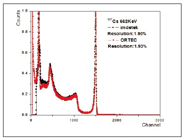
PAM-PA01 series are pixel electrode structured detectors based on CZT crystal. They can detect X-ray, γ-ray and imaging. They have a high energy and space resolution.
1. Specification of CZT High Resolution Pixel Detector
Material
CdZnTe
Density
5.8g/cm3
Volume resistance
>1010Ω.cm
Dimensions
10.0×10.0mm2
Thickness
2.0mm
5.0mm
Pixel size
1.1×1.1mm2
Pixel array
8×8
Electrode material
Au
Operation temperature
-20℃-+40℃
Energy range
20KeV~700MeV
20KeV~700MeV
Energy resolution(22℃)
<6%@59.5KeV
<4.5%@122KeV
<3%@662KeV
Defective pixel(DP)
10℃~40℃
Storage temperture
20%-80%
Remarks
Customized available
2. Spectrum of [...]
2019-04-24meta-author
Hybrid Chips of Gallium Nitride and Silicon
Researchers at MIT say they’ve made a big step toward combining the capabilities of the silicon used in computer chips with properties of the compound semiconductors found in lasers and high-powered electronics. In the October issue of IEEE Electron [...]