PAM-XIAMEN offers PSS patterned sapphire substrate for high brightness GaN based LED EPI growing application. The patterned sapphire substrate wafer consiste en hacer crecer una máscara de grabado en seco sobre el sustrato de zafiro. La máscara está grabada mediante un proceso de fotolitografía estándar. Luego, el zafiro se graba con la tecnología de grabado ICP y, mientras tanto, se quita la máscara. Después de eso, el material de GaN se hace crecer en el zafiro, de modo que la epitaxia vertical del material de GaN se convierte en la epitaxia horizontal. Los detalles del sustrato de zafiro estampado se encuentran a continuación:
Sustrato de zafiro PSS
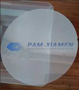
1.Sspecificacioness Sustrato de zafiro estampado
| Parámetros | Especificaciones | Unidad |
| Materiales | Monocristalina Al2O3 de alta pureza | |
| Diámetro | 50,8 ± 0,1 | ㎜ |
| Espesor | 430 ± 10 | ㎛ |
| Variación de espesor total | ≤10 | ㎛ |
| Longitud plana primaria | 16,0 ± 1,0 | ㎜ |
| Orientación plana primaria | Un plano ± 0,2 | |
| Calidad de la superficie frontal | Preparado para epitaxial | |
| Rugosidad de la superficie trasera | 1,0 ± 0,1 | ㎛ |
| Orientación de la superficie A | 0˚apagado ± 0,1 | |
| Orientación de superficie M | 0,2˚apagado ± 0,10 | |
| Orientación de la superficie R | R9 | |
| ARCO | -10 ~ 0 | ㎛ |
| DEFORMACIÓN | ≤15 | ㎛ |
| Ancho del patrón | 2,7 ± 0,15 | ㎛ |
| Altura del patrón | 1,7 ± 0,15 | ㎛ |
| Paso del patrón | 3,0 ± 0,05 | ㎛ |
2.¿Por qué elegir un sustrato de zafiro estampado para LED?
On the one hand, the cone-shaped patterned sapphire substrate wafer can effectively reduce the dislocation density of the GaN epitaxial material(the patterned sapphire substrate dislocation is low), thereby reducing the non-radiative recombination of the active area, reducing the reverse leakage current, and improving the life of the LED. On the other hand, the light emitted from the active region is scattered multiple times by the interface of GaN and sapphire substrate, and the exit angle of total reflection light is changed, increasing the probability that the light of the flip-chip LED emerges from the sapphire substrate, thereby improving the extraction efficiency of the light.
En resumen, el brillo de la luz emitida por el LED que crece sobre el sustrato de zafiro con patrón nano es mucho mejor que el del LED tradicional. La corriente de fuga inversa se reduce, lo que prolonga la vida útil del LED.
A patterned sapphire substrate belongs to the semiconductor industry. As a high-brightness epitaxial material, it is the source material of the LED lighting industry. Meanwhile, using PSS Al2O3 wafer to grow epitaxial wafers is the most effective way to improve the brightness of the chip. It is also the best choice for the high-power and high-brightness epitaxial wafers.

Para obtener más información, contáctenos por correo electrónico a victorchan@powerwaywafer.com ypowerwaymaterial@gmail.com.