PAM XIAMEN offers 2 inch AlN on sapphire wafer grown by MOCVD, which is the major technology for growing single-crystal aluminum nitride onto large-size, low-cost, and mature sapphire substrate. One important utilization of high-quality AlN-on-sapphire template is the deep ultraviolet (DUV) optoelectronic devices.
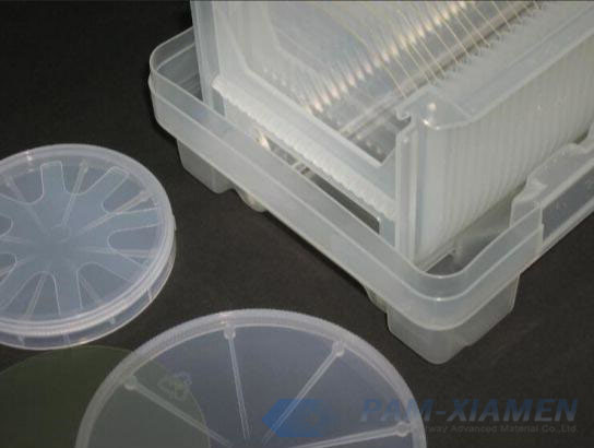
1. Specification of AlN Template on Sapphire
Spec1:
2 INCH ALUMINUM NITRIDE ALN TEMPLATE ON SAPPHIRE (0001) SEMI-INSULATING TYPE
type de conductivité: AlN semi-isolant
Substrate: Sapphire
Dimension: Φ50.8 mm ± 0.1 mm
Thickness: 200nm ~ 5 um (4000~5000 nm)
Edge Exclusion Zone: < 2 mm
Usable area: >90%
Orientation: C plane (0001) ± 1°
Total Thickness Variation: <15 μm
Crystallinity: XRD FWHM of (0002) < 350 arcsec
XRD FWHM of (10-12) < 450 arcsec
Surface Roughness Ra <5 nm (10 µm x 10 µm)
Substrate Structure: Sapphire (0001)
Polishing: Single side polished (SSP). Double-side polished (DSP) are available upon request.
About the usable area: The calculation method refers to the area that can be used after removing the defects (such as pits) whose macro-size is more than 0.2mm.
Spec2:
| Template Name | AlN on Sapphire Wafer |
| Substrat | 2” & 4”Sapphire |
| Substrate thickness | 430~450um |
| AlN Thickness | 50~ 400nm+/-10nm |
| Template Size | 2inch,4inch |
| Surface Roughness | Ra < 1 nm |
| FWHM (002) | 0.17° |
Features of AlN/Sapphire:
High uniformity and crystal quality
2. Characterization Test of Aluminum Ntride on Sapphire Wafer
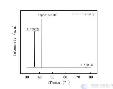
XRD spectra of 2-inch Aluminum Nitride films on sapphire
There only c-axis orientation with sharp peak of Aluminum Nitride films on Sapphire.
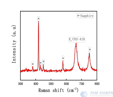
Raman spectra of 2” single crystal AlN films on Sapphire.
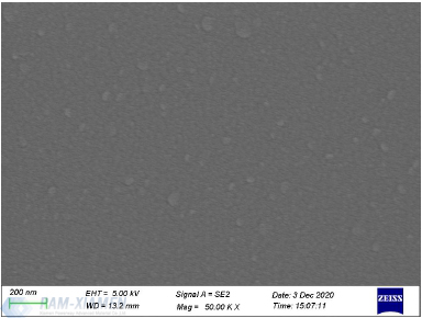
SEM micrographs (×50.00KX) of the 2-inch AlN epilayers grown on sapphire.
AFM micrographs of the AlN films on sapphire after rough polishing.
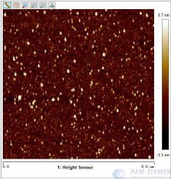
Image Ra =0.727 nm with the scanning area of 5×5 μm2.
3. Growth Difficulties and Solutions for Epitaxial AlN Thin Film Deposited by MOCVD
Generally, an AlN grows epitaxially on a C-plane sapphire substrate. However, it is very difficult to prepare high-quality epitaxial AlN on C-plane sapphire. In addition to the large AlN / sapphire lattice mismatch and thermal mismatch, there are two reasons:
- The Al-N bond is very strong. The diffusion of Al atoms on the growth surface is limited, and the lateral growth rate is very low, and it is difficult to form two-dimensional layered growth;
- There is a strong pre-reaction between the Al source TMA and NH in the MOCVD growth. The pre-reaction will not only consume a large amount of reactants, but the solid adducts formed may be deposited on the surface of the wafer and cannot be fully decomposed, resulting in the doping of impurities in the AlN epitaxy, even causing polycrystalline growth of the epitaxial layer, which seriously affects the improvement of device performance
Solutions are proposed for obtaining high quality epitaxial thin film deposited by MOCVD:
On the one hand, because of the growth characteristics of AlN itself, when the thickness of AlN on sapphire is too thin (eg. 1um), a large number of uncombined areas will be formed on the surface. It is suggested to increase the thickness of aluminium nitride properly if a better surface atomic step is needed.
On the other hand, during the growth of AlN, the in-situ temperature modulation method can be introduced to form an interface layer in the AlN material, which played a role in annihilating dislocations and releasing stress. This method is time-saving and labor-saving, simple and easy to implement, and will not cause contamination of the reaction chamber. It is an effective method to improve the quality of AlN layer deposited on sapphire.
4. Applications of AlN on Sapphire Template
Aluminum nitride (AIN), as an ultra-wide band gap semiconductor material, is an important ultraviolet light-emitting material with the advantages of ultra-high breakdown field strength, high saturation electron drift velocity, high thermal conductivity, high surface sound velocity, high nonlinear optical coefficient, etc. So epitaxial aluminum nitride film grown on sapphire substrate has important applications in ultraviolet detectors, ultraviolet light-emitting diodes and ultraviolet lasers, especially in back-incident daylight blind detectors, and inverted-packaged ultraviolet LEDs. Besides, it can be for piezoelectric applications with bulk acoustic waves.
For more information, please contact us email at victorchan@powerwaywafer.com and powerwaymaterial@gmail.com

