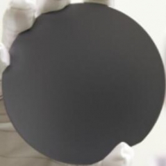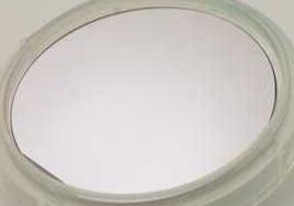

GaN à base de LED épitaxiales Wafer
GaN de PAM-XIAMEN (nitrure de gallium) à base de plaquette épitaxiale de LED est de très haute luminosité de lumière bleue et verte diodes électroluminescentes (LED) et des diodes laser d'application (LD).
- La description
Description du produit
La plaquette épitaxiale LED est un substrat chauffé à une température appropriée. Le matériau des plaquettes LED est la pierre angulaire du développement technologique pour l’industrie de l’éclairage à semi-conducteurs. Différents matériaux de substrat nécessitent différentes technologies de croissance de tranches épitaxiales LED, technologies de traitement de puces et technologies d'emballage de dispositifs différentes. Le substrat pour plaquette épi LED détermine la voie de développement de la technologie d’éclairage à semi-conducteurs. Pour obtenir une efficacité lumineuse, les fournisseurs de plaquettes épitaxiales accordent plus d'attention aux plaquettes épitaxiales à LED à base de GaN, car le prix des plaquettes épitaxiales est faible et la densité de défauts des plaquettes épi est faible. L'avantage de la plaquette épi LED sur le substrat GaN est la réalisation d'un rendement élevé, d'une grande surface, d'une lampe unique et d'une puissance élevée, ce qui simplifie la technologie de processus et améliore le taux de rendement élevé. Les perspectives de développement du marché des plaquettes LED épi sont optimistes.
1. Liste des plaquettes LED
|
Plaquette épitaxiale LED |
||||||||
| Article | Taille | Orientation | Émission | Longueur d'onde | Épaisseur | Substrat | Surface | Surface utilisable |
| PAM-50-LED-BLEU-F | 50mm | 0°±0,5° | lumière bleue | 445-475nm | 425um +/-25um | Saphir | PL | >90% |
| PAM-50-LED-BLEU-PSS | 50mm | 0°±0,5° | lumière bleue | 445-475nm | 425um +/-25um | Saphir | PL | >90% |
| PAM-100-LED-BLEU-F | 100mm | 0°±0,5° | lumière bleue | 445-475nm | / | Saphir | PL | >90% |
| PAM-100-LED-BLEU-PSS | 100mm | 0°±0,5° | lumière bleue | 445-475nm | / | Saphir | PL | >90% |
| PAM-150-LED-BLEU | 150mm | 0°±0,5° | lumière bleue | 445-475nm | / | Saphir | PL | >90% |
| PAM-100-LED-BLEU-SIL | 50mm | 0°±0,5° | lumière bleue | 445-475nm | / | Silicium | PL | >90% |
| PAM-100-LED-BLEU-SIL | 100mm | 0°±0,5° | lumière bleue | 445-475nm | / | Silicium | PL | >90% |
| PAM-150-LED-BLEU-SIL | 150mm | 0°±0,5° | lumière bleue | 445-475nm | / | Silicium | PL | >90% |
| PAM-200-LED-BLEU-SIL | 200mm | 0°±0,5° | lumière bleue | 445-475nm | / | Silicium | PL | >90% |
| PAM-50-LED-VERT-F | 50mm | 0°±0,5° | lumière verte | 510-530nm | 425um +/-25um | Saphir | PL | >90% |
| PAM-50-LED-VERT-PSS | 50mm | 0°±0,5° | lumière verte | 510-530nm | 425um +/-25um | Saphir | PL | >90% |
| PAM-100-LED-VERT-F | 100mm | 0°±0,5° | lumière verte | 510-530nm | / | Saphir | PL | >90% |
| PAM-100-LED-VERT-PSS | 100mm | 0°±0,5° | lumière verte | 510-530nm | / | Saphir | PL | >90% |
| PAM-150-LED-VERT | 150mm | 0°±0,5° | lumière verte | 510-530nm | / | Saphir | PL | >90% |
| PAM-100-LED-ROUGE-GAAS-620 | 100mm | 15°±0,5° | lumière rouge | 610-630nm | / | AsGa | PL | >90% |
| PAM210527-LED-660 | 100mm | 15°±0,5° | lumière rouge | 660 nm | / | AsGa | PL | >90% |
| PAM-210414-850nm-LED | 100mm | 15°±0,5° | IR | 850 nm | / | AsGa | PL | >90% |
| PAMP21138-940LED | 100mm | 15°±0,5° | IR | 940 nm | / | AsGa | PL | >90% |
| PAM-50-LED-UV-365-PSS | 50mm | 0°±0,5° | UVA | 365 nm | 425um +/-25um | Saphir | ||
| PAM-50-LED-UV-405-PSS | 50mm | 0°±0,5° | UVA | 405 nm | 425um +/-25um | Saphir | ||
| PAM-50-LED-UVC-275-PSS | 50mm | 0°±0,5° | UVC | 275 nm | 425um +/-25um | Saphir | ||
| PAM-50-LD-UV-405-SIL | 50mm | 0°±0,5° | UV | 405 nm | / | Silicium | PL | >90% |
| PAM-50-LD-BLEU-450-SIL | 50mm | 0°±0,5° | lumière bleue | 450 nm | / | Silicium | PL | >90% |
As a LED epitaxial wafer manufacturer, PAM-XIAMEN can offer activated and unactivated GaN Epi LED wafer for LED and laser diodes (LD) application,such as For micro LED or ultra thin wafer or UV LED researches or LED manufacturers. LED epitaxial wafer on GaN is grown by MOCVD with PSS or flat sapphire for LCD back light, mobile, electronic or UV(ultraviolet), with blue or green or red emission, including InGaN/GaN active area and AlGaN layers with GaN well/AlGaN barrier for different chip sizes.
2. InGaN/GaNPlaquette épitaxiale LED à base de nitrure de gallium
GaN sur Al2O3-2” wafer epi Specification (plaquette LED épitaxiales)
| Blanc : 445 ~ 460 nm |
| Bleu : 465 ~ 475 nm |
| Vert : 510 ~ 530 nm |
1. Technique de croissance - MOCVD
2.Wafer diamètre: 50,8 mm
Matériau du substrat 3.Wafer : substrat saphir à motifs (Al2O3) ou saphir plat
4.Wafer taille de motif: 3X2X1.5μm
3. Structure de la plaquette :
| Structure de couches | Épaisseur (μm) |
| p-GaN | 0.2 |
| p-AlGaN | 0.03 |
| InGaN / GaN (Région actif) | 0.2 |
| n-GaN | 2.5 |
| u- GaN | 3.5 |
| Al2O3 (substrat) | 430 |
4. Paramètres des plaquettes pour fabriquer des puces :
| em | Couleur | Taille de puce | Caractéristiques | Apparition | |
| PAM1023A01 | Bleu | 10mil x 23mil |  |
Éclairage | |
| Vf = 2,8 ~ 3.4V | LCD rétro-éclairage | ||||
| Po = 18 ~ 25mW | appareils mobiles | ||||
| Dv 450 ~ 460nm | électronique grand public | ||||
| PAM454501 | Bleu | 45mil x 45mil | Vf = 2,8 ~ 3.4V |  |
éclairage général |
| Po = 250 ~ 300mW | LCD rétro-éclairage | ||||
| Dv 450 ~ 460nm | affichage extérieur |
5. Application de la plaquette épitaixale LED :
*Si vous avez besoin d'informations plus détaillées sur la plaquette épitaxiale à LED bleue, veuillez contacter notre service commercial.
Éclairage
LCD rétro-éclairage
appareils mobiles
électronique grand public
6. Spécification de LED Epi Wafer à titre d'exemple :
Spécification PAM190730-LED
– taille : 4 pouces
– WD : 455 ± 10nm
– luminosité : > 90mcd
– VF : < 3,3V
– Épaisseur n-GaN : <4.1㎛
– épaisseur u-GaN : <2.2㎛
– substrat : substrat saphir à motifs (PSS)
7. Matériau de la plaquette LED à base de GaAs (arséniure de gallium) :
En ce qui concerne la plaquette LED GaAs, elles sont cultivées par MOCVD, voir ci-dessous longueur d'onde de GaAs plaquette LED:
Rouge: 585nm, 615 nm, 620 ~ 630nm
Jaune : 587 ~ 592 nm
Jaune/Vert : 568 ~ 573 nm
8. Définition de la plaquette épitaxiale LED :
Ce que nous proposons est une plaquette épi LED nue ou une plaquette non traitée sans processus de lithographie, contacts n- et métalliques, etc. Et vous pouvez fabriquer la puce LED à l'aide de votre équipement de fabrication pour différentes applications telles que la recherche en nano-optoélectronique.
Remarque:
Le gouvernement chinois a annoncé de nouvelles limites à l'exportation de matériaux au gallium (tels que GaAs, GaN, Ga2O3, GaP, InGaAs et GaSb) et aux matériaux au germanium utilisés pour fabriquer des puces semi-conductrices. À compter du 1er août 2023, l’exportation de ces matériaux n’est autorisée que si nous obtenons une licence du ministère chinois du Commerce. J'espère votre compréhension et votre coopération !
Pour ces détails caractéristiques GaAs plaquette LED, visitez s'il vous plaît:GaAs Epi Wafer pour LED
Pour les spécifications LED UV gaufrettes, visitez s'il vous plaît:LED UV Epi Wafer
Pour la tranche LED sur les spécifications de silicium, visitez s'il vous plaît:LED Wafer sur silicium
Blue GaN LD spécifications Wafer, visitez s'il vous plaît: Bleu GaN LD Wafer
Pour la plaquette Violet GaN LD, veuillez visiter :Plaquette de diode laser GaN 405 nm
Plaquette LED infrarouge 850 nm et 940 nm
Plaquette épi LED AlGaAs/GaAs infrarouge rouge 850-880 nm et 890-910 nm
Plaquettes GaN pour fabriquer des dispositifs LED
Epitaxie de Structure LED GaN sur Substrat Saphir Plat ou PSS
Croissance épitaxiale GaN sur saphir pour LED
Structure du photodétecteur PIN GaN à base de Si
Pour plus de services de fonderie, veuillez visiter :Services de fonderie GaN pour la fabrication de LED
Vous aimerez aussi ...
-
GaAs tranches épitaxiées
PAM-XIAMEN fabrique divers types de matériaux semi-conducteurs de type n dopés au silicium épi III-V à base de Ga, Al, In, As et P cultivés par MBE ou MOCVD. Nous fournissons des structures d'épiwafer GaAs personnalisées pour répondre aux spécifications des clients. Veuillez nous contacter pour plus d'informations.
-
GaN HEMT TRANCHE ÉPITAXIALE
Les HEMT (transistors à haute mobilité électronique) en nitrure de gallium (GaN) constituent la nouvelle génération de technologie de transistor de puissance RF. Grâce à la technologie GaN, PAM-XIAMEN propose désormais AlGaN/GaN HEMT Epi Wafer sur saphir ou silicium, et AlGaN/GaN sur modèle saphir.
-
plaquette InSb
PAM-XIAMEN propose une plaquette InSb à semi-conducteur composé – une plaquette d'antimonide d'indium qui est cultivée par LEC (Liquid Encapsulated Czochralski) en tant que qualité épi-prête ou mécanique avec type n, type p ou semi-isolant dans différentes orientations (111) ou (100). L'antimonide d'indium dopé avec de l'isoélectronique (tel que le dopage N) peut réduire la densité des défauts pendant le processus de fabrication de couches minces d'antimonure d'indium.
-
Substrat SiC Wafer
La société dispose d'une ligne complète de production de substrats de plaquettes SiC (carbure de silicium) intégrant la croissance cristalline, le traitement des cristaux, le traitement des plaquettes, le polissage, le nettoyage et les tests. Aujourd'hui, nous fournissons des plaquettes SiC commerciales 4H et 6H avec semi-isolation et conductivité sur axe ou hors axe, tailles disponibles : 5x5 mm2, 10x10 mm2, 2", 3", 4", 6" et 8", perçant des technologies clés telles que comme la suppression des défauts, le traitement des germes de cristal et la croissance rapide, favorisant la recherche et le développement fondamentaux liés à l'épitaxie du carbure de silicium, aux dispositifs, etc.
-
Modèles GaN
Modèle de PAM-XIAMEN produits sont constitués de couches cristallines de (nitrure de gallium) des modèles de GaN (nitrure d'aluminium) modèle AlN, (nitrure de gallium d'aluminium) modèles AlGaN et (indium du nitrure de gallium) modèles InGaN, qui sont déposés sur saphir -
Cz monocristallins Silicon
PAM-XIAMEN, un producteur de silicium monocristallin en vrac, peut proposer des tranches de silicium monocristallin <100>, <110> et <111> avec un dopant N&P de 76,2 à 200 mm, qui sont cultivées par la méthode CZ. La méthode Czochralski est une méthode de croissance cristalline, appelée méthode CZ. Il est intégré dans un système thermique à tube droit, chauffé par une résistance en graphite, fait fondre le polysilicium contenu dans un creuset en quartz de haute pureté, puis insère le cristal germe dans la surface de la masse fondue pour le soudage. Après cela, le cristal germe en rotation est abaissé et fondu. Le corps est infiltré et touché, progressivement soulevé et fini ou tiré à travers les étapes de striction, de striction, d'épaulement, de contrôle du diamètre égal et de finition.
-
Ge (germanium) cristaux simples et Wafers
PAM-XIAMEN propose des plaquettes de germanium de 2", 3", 4" et 6", qui est l'abréviation de plaquette Ge cultivée par VGF / LEC. Une plaquette de germanium de type P et N légèrement dopée peut également être utilisée pour l'expérience à effet Hall. À température ambiante, le germanium cristallin est fragile et peu plasticisé. Le germanium a des propriétés semi-conductrices. Le germanium de haute pureté est dopé avec des éléments trivalents (tels que l'indium, le gallium, le bore) pour obtenir des semi-conducteurs en germanium de type P ; et des éléments pentavalents (tels que l'antimoine, l'arsenic et le phosphore) sont dopés pour obtenir des semi-conducteurs en germanium de type N. Le germanium possède de bonnes propriétés semi-conductrices, telles qu'une mobilité élevée des électrons et une mobilité élevée des trous. -
substrat autoportant de GaN
PAM-XIAMEN a mis en place la technologie de fabrication pour autoportante (nitrure de gallium) plaquette de substrat de GaN, qui est pour UHB-LED et LD. Par épitaxie en phase vapeur d'hydrure (HVPE) technologie, notre substrat de GaN a une faible densité de défauts.