Silicon carbide has a variety of crystal types, but the silicon crystal structure the market needed is mainly 4H-SiC. So the silicon carbide crystal growth in crystal types is a defect. To a certain extent, it can be distinguished by the naked eye. A more accurate measurement method for testing the silicon carbide crystal distribution is Raman spectroscopy: Raman spectroscopy has characteristics for crystals, and the peak positions of the light emitted by different crystals are different.
1. What is Raman Spectroscopy?
En 1928, le scientifique indien Raman a découvert la diffusion Raman dans l'expérience d'étude du spectre de diffusion du benzène liquide. La spectroscopie de diffusion Raman, en termes simples, consiste à utiliser un faisceau de lumière incident sur une substance, la fréquence de la lumière incidente est v et la fréquence de la lumière diffusée résultante sera v, v + Δv1, v-Δv1, v + Δv2, v-Δv2, etc. Ces Δv1, Δv2, etc. Δv ont des caractéristiques. En d'autres termes, chaque substance a une certaine différence (position du pic, intensité du pic), qui est appelée décalage Raman (la lumière émise moins la lumière incidente).
Par exemple, le spectre Raman de 4H-SiC est:
| Décalage Raman (cm-1) | Onde acoustique transversale E2 | Onde acoustique transversale E2 | Onde acoustique transversale A1 | Onde acoustique transversale E2 | Onde acoustique transversale A1 | Onde acoustique longitudinale A1 | LOPC | LOPC |
| 4H-SiC | 194.958 | 204.034 | 610.031 | 776.489 | 796.861 | 963.106 | 964.769 | 994.643 |
The table above shown here is the Raman shift. During the silicon carbide crystal distribution measurement, the computer will help to calculate it and process it as a Raman shift spectrum.
2. How to Test the Silicon Carbide Crystal Distrubution?
Les conditions de test typiques sont les suivantes: en utilisant le laser 532 nm du laser Ar + du spectromètre LabRAM HR Raman, il est incident verticalement, la puissance d'excitation est de 200 mW et le mode de collecte de la lumière diffusée est le mode de rétrodiffusion. La lumière incidente avec différentes longueurs d'onde a différentes profondeurs de pénétration. Généralement, le laser 266 nm est de 0,2 um, le laser de 325 nm est de 2 um et le laser de 514 nm est de 30 um, ce qui signifie que la lumière ultraviolette ne peut être utilisée que pour mesurer des échantillons minces.
Because the silicon carbide wafer has different positions, multiple measurements will be taken to obtain the silicon carbide crystal distribution:
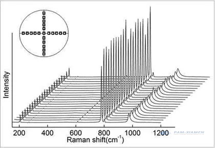
The data has three indicators: the position of the peak, the height of the peak (light intensity), and the width of the peak. Only when the peak position is completely matched, can it be le 4H-SiC qualifié. Comme pour la DRX, chaque fois qu'il y a d'autres pics, ce sont des substances d'autres phases, ce qui est un défaut.
The difference in the position of the peak is due to the difference in the energy of the phonons brought about by the different silicon carbide crystal lattices, that is, the different frequencies. Each phonon has its corresponding energy level. The virtual energy level theory can be used to explain Raman (non-linear process):
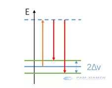
La particule absorbe la lumière incidente jusqu'au niveau d'énergie virtuelle (orange), puis revient à un niveau d'énergie vibratoire (rouge) différent du niveau d'énergie d'origine. Parce que le niveau d'énergie supérieur est un niveau d'énergie virtuelle, la fréquence de la lumière incidente peut être modifiée, tant qu'elle n'est pas en conflit avec le niveau d'énergie réel d'origine.
Il est à noter que le mode LOPC (964,769 cm-1) peut être utilisé pour analyser la concentration de porteurs:
n = 1.25 * 1017cm-2 *(964.769cm-1-VLOPC measurement)
As the carrier concentration increases, the interaction between atoms and the lattice increases, which makes the Raman peak blue shift (smaller), the intensity decreases, and the width increases. This method is not as accurate as other methods and can only be used as an aid to analyze the silicon carbide crystal distribution.
3. Why not Use XRD to Measure Silicon Carbide Crystal Distribution?
X-rays are optical radiation generated by the transition of electrons in the inner layer of atoms under the bombardment of high-speed moving electrons, including continuous X-rays and characteristic X-rays. Silicon carbide single crystal can be used as X-ray gratings, and the coherent scattering produced by these large numbers of particles (atoms, ions, or molecules) will cause light interference, increasing or decreasing the intensity of scattered X-rays. Due to the superposition of scattered waves from a large number of particles, the beams that interfere with each other to produce the highest intensity are called X-ray diffraction lines.
Pour répondre aux conditions de diffraction, la formule de Bragg peut être appliquée: 2dsinθ = nλ.
Le faisceau incident amène chaque diffuseur à réémettre une petite partie de son intensité sous forme d'onde sphérique. Si les diffuseurs sont disposés symétriquement avec l'intervalle d, ces ondes sphériques ne seront synchronisées que dans le sens où leur différence de longueur de trajet 2dsinθ est égale à un multiple entier de la longueur d'onde λ. Dans ce cas, une partie du faisceau incident est déviée d'un angle de 2θ, ce qui produira des points de réflexion dans le diagramme de diffraction.
Use X-rays of known wavelengths to measure the θ angle to calculate the interplanar spacing d, which is used for X-ray structure analysis; the other is to use a silicon carbide seed crystal with a known d to measure the θ angle to calculate the characteristic X-ray wavelength, and then the elements contained in the sample can be found in the existing data.
The measurement formula is 2dSinθ=λ. While the d value among the cubic silicon carbide crystal is close, and the characteristic is not obvious enough, the accurate silicon carbide crystal distribution cannot be precisely determined. For these reasons, it is not suitable to use the XRD to measure the distribution of silicon carbide crystals.

Pour plus d'informations, veuillez nous contacter par e-mail à victorchan@powerwaywafer.com et powerwaymaterial@gmail.com.